
What Is Auger Electron Spectroscopy (AES)?
Energy doesn’t stay put, and Auger Electron Spectroscopy (AES) proves it. When a high–energy electron beam strikes an atom, it ejects a tightly bound core electron, creating a vacancy. An outer-shell electron drops in to occupy this vacancy, and instead of releasing the energy as light, it transfers it to a third electron, which is ejected from the atom: the Auger electron. This electron carries element-specific kinetic energy, acting like a chemical fingerprint of the material.
Also known as Auger Spectroscopy, Auger Emission Spectroscopy, Auger electron analysis, or simply AES, this technique is indispensable for ultra-sensitive surface characterization. It’s ideal for detecting surface contamination, characterizing thin films, monitoring oxide layers, and evaluating interfaces, all with nanometer-scale precision.
At Covalent, AES is our cornerstone technique for analyzing the outermost layers of a material. Whether you are troubleshooting surface defects or validating thin film integrity, our AES labs deliver fast, precise, and actionable data for your materials development pipeline.
High Resolution
Surface Sensitivity
Elemental Fingerprinting
Why Use AES?
AES is engineered to explore the most important elements of surface chemistry. Its elemental sensitivity and ultra-thin probing depth make it the method of choice for analyzing thin films, nanostructures, and coatings.
AES also enables rapid surface composition measurements and, when paired with ion sputtering, powerful depth profiling for layer‑by‑layer mapping.
Ultra-Precise Analysis
Thin Film Validation
Cross-Industry Impact
How Auger Electron Spectroscopy Measurement Works
AES operates by scanning a material’s surface with a focused beam of high-energy electrons, typically ranging between 3 to 30 keV. This knocks out a tightly bound inner-shell electron, creating an inner-shell vacancy. An outer-shell electron fills the gap, and the excess energy ejects a third electron, known as an Auger electron.
These Auger electrons have kinetic energies specific to their element and are independent of the beam’s energy. By measuring them, AES produces a spectral “signature” with peaks labeled as KLM, KLL, or LMM, notations that denote the shells involved in the transition.
Because only electrons emitted from the uppermost 0.5-10 nm of the surface can escape without losing energy, AES is one of the most surface-sensitive techniques available. That’s why all AES measurements are conducted in ultra-high vacuum (UHV), to retain the signal purity and avoid atmospheric interference.
Our specialists at Covalent decode these spectral signatures to trace contamination, map elemental diffusion, and investigate surface-level anomalies across industries.
Equipment Used for AES

PHI 710 Scanning Auger Nanoprobe
- Imaging of textured or curved samples without analyzer-induced shadowing, enabled by the PHI’s coaxial electron gun-analyzer technology.
- Monoatomic argon (Ar⁺) sputter depth profiling for compositional analysis through layered structures.
- Maximum sample size of 60 mm diameter and 20 mm thickness.
- Inert sample transfer for air-sensitive materials.
- Maximum electron beam accelerating voltage of 25 kV.
- Sample must be a solid and compatible with ultra-high vacuum (no liquid).
Key Differentiators
AES is where atomic-level precision meets unmatched clarity.
| Property | AES |
|---|---|
| Surface Sensitivity | Probes the topmost ~0.5-10 nanometers. Ideal for ultra-thin surface analysis |
| Elemental Detection | Detects all elements except Hydrogen (H) and Helium (He) |
| Lateral Resolution | Achieves 10-30 nm resolution |
| Depth Profiling | Available via ion sputtering for compositional layer-by-layer insights |
| Quantification | Semi-quantitative to quantitative results |
| Chemical State Info | Limited (can consult for XPS) |
| Vacuum Requirement | Requires UHV |
| Sample Compatibility | Ideal for conductive solids. Insulator can be thinly coated with conductive layer |
| Sample Damage Risk | Soft or organic layers may be susceptible |
Strengths
Think of AES as a lie detector for surfaces. It interrogates only the few top level atomic layers, with unmatched precision.
Other Strengths of AES:
- Depth Profiling: In combination with ion sputtering, AES provides layer‑by‑layer elemental mapping for multilayer stacks, ideal in failure analysis and thin‑film studies.
- Versatile Applications: Supports contamination analysis, corrosion layer evaluation, and grain boundary mapping across sectors from biomedical to aerospace.
- At Covalent, we push this power to deliver multi-modal datasets by integrating AES with complementary techniques like XPS and SEM.
Limitations
AES is a powerful tool, but a one-size-fits-all approach doesn’t fit all materials. Here is when AES may not be ideal:
- AES is not suitable for Hydrogen and Helium due to the lack of usable Auger transitions.
- AES only works well with coated and conductive surfaces.
- Tests are conducted in ultra-high vacuum. Therefore, volatile and moisture-sensitive materials will require special handling.
- Not the ideal technique to investigate oxidation states or chemical bonding (at Covalent, we’d use XPS for this).
- Polymers and low-density films can be damaged due to prolonged electron exposure or ion sputtering.
- Should be paired with ToF-SIMS or EDS for deeper material insights.
We recommend consulting an expert at Covalent for evaluating each sample’s characteristics and project goals before defining the right analytical pathway.
Example Outputs
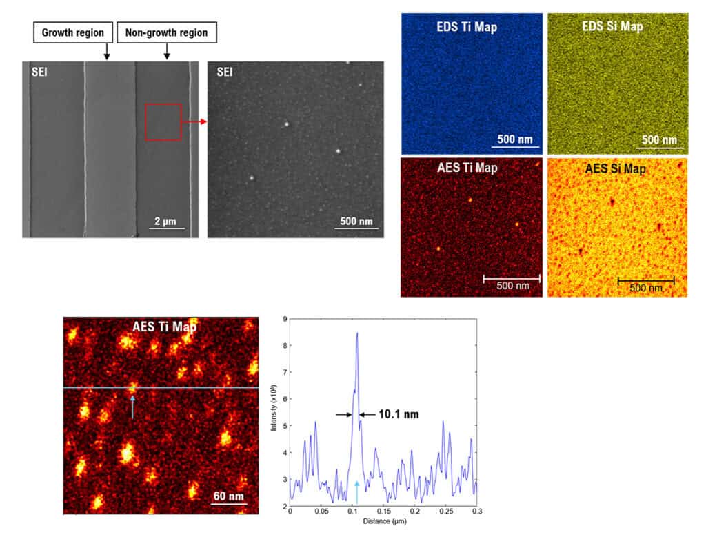
Area selective deposition (ASD) is a critical technique in advanced semiconductor manufacturing, enabling sub-10 nm patterning through iterative atomic layer deposition (ALD) and atomic layer etching (ALE) cycles. However, process-induced selectivity loss, where material unintentionally grows in non-growth regions, can lead to device failure.
In this ASD example, TiO₂ was deposited on SiO₂-patterned surfaces using ALD and ALE cycles. Scanning electron microscopy (SEM) revealed nanoscale particles in the non-growth regions that were not readily visible in energy-dispersive X-ray spectroscopy (EDS) maps. The EDS maps showed uniform titanium and silicon signal intensities.
Auger electron spectroscopy (AES), performed using the PHI 710 Scanning Auger Nanoprobe, provided high-resolution chemical mapping and identified the defect particles as titanium. A line scan of the Ti signal across a different analysis area on the ALD/ALE sample further confirmed the presence of 10 nm titanium particles.
This example highlights the AES’ capability to characterize nanoscale defects providing essential insight into ALD/ALE process control and failure mechanisms.
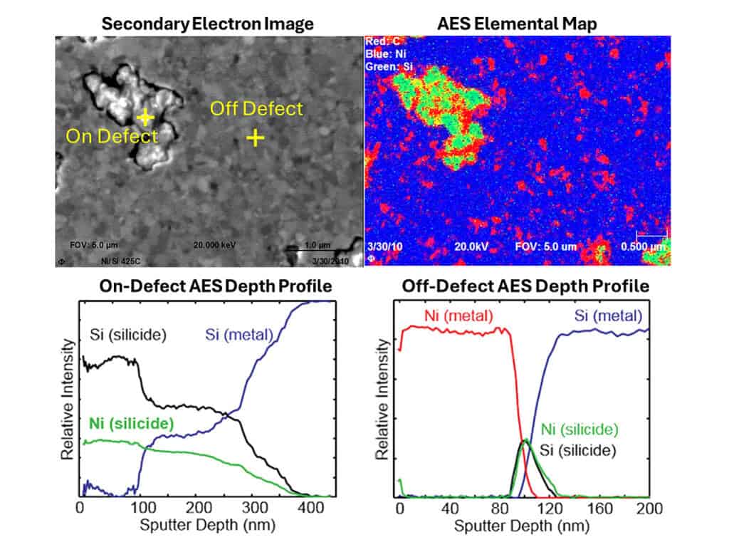
Sample Requirements
To ensure accurate results, AES samples must meet the following criteria:
- Must be vacuum-compatible, dry, and solid.
- The best fit is flat, conductive and thinly coated insulators.
- The sample size should typically be up to 25 x 25 mm.
- Small particles or powders are best mounted on a substrate or a stub.
- Avoid moisture and organics as they interfere with the vacuum and signals.
AES Applications by Industry
Semiconductor
Nanometer‑precision interface chemistry, contamination control, and process validation.
Aerospace & Energy
Protective coating integrity, oxidation monitoring, and degradation tracking under stress.
Medical Devices
Surface cleanliness, biocompatibility validation, and passivation layer verification.
Advanced Manufacturing
Identifies trace contaminants in additive and precision builds to safeguard material performance.
Techniques That Complement AES
AES, when paired with deeper or more chemically detailed tools, expands the scope of surface-level investigation.
Complements AES by offering deeper probing (~5-10 nm) and richer state information. While AES excels at spatial resolution, XPS wins on quantification. But together, they cover more depth and detail.
AES Testing Services at Covalent
AES analysis at Covalent is delivered through Covalent Connect, our network of trusted partner labs. You get access to high-resolution Auger electron spectroscopy without finding, vetting, and managing another lab. Our scientists scope your project, coordinate the analysis, and stay your single point of contact from quote to final report.
Where Covalent adds the most value is in what happens around the measurement. We help define the right analytical approach for your thin films, interfaces, or surface defects. We then correlate AES results with complementary techniques like SEM, XPS, and ToF-SIMS, so you get a complete answer instead of a single dataset. If your failure analysis or process validation question lives in the top 10 nanometers, we’ll bring the right tools together to answer it.
Every project comes with one consolidated report, expert interpretation, and the same strict confidentiality and IP protection you expect from Covalent. Ready to understand your surfaces at the level they operate? Talk to a Covalent scientist about your AES project.
Frequently Asked Questions
What kind of samples can be analyzed with AES?
Is AES destructive?
Can AES be used on non-conductive materials?
What is the difference between AES and XPS?
AES has better lateral resolution; XPS gives chemical state and better quantification, which the page already says.