
What Is 2D X-Ray Inspection?
2D X-ray inspection is a non-destructive failure analysis method that captures hidden faults in the PCBs and BGA solder joints.
Key benefit:
It offers rapid defect detection in PCB X-ray inspection and BGA X-ray inspection, catching hidden failures such as voids, cracks, or Head in Pillow defects without destructive cross-sectioning.
Efficient Inspection
Fast and Non-destructive
High Clarity
Why Use 2D X-Ray Inspection?
2D X-ray inspection is a fast, non-destructive approach that adds depth perception for exposing hidden defects in modern electronics. It delivers high-resolution insights into solder voids, cracks, and interconnect failures. It supports high-throughput PCBA inspection services without damaging or altering fragile assemblies. It is well-suited for multilayer PCBs, BGAs, and high-density packaging.
Improved Defect Visibility
High-Magnification and Resolution
Flexible Energy Range
How 2D X-Ray Inspection Works
- An X-ray source projects radiation through the sample at multiple tilt angles.
- By tilting or rotating the sample, the system captures angled projections that reduce feature overlap and reveal clearer details of hidden structures.
- Denser regions absorb more radiation (appearing darker), while lighter regions allow greater transmission.
- Highly effective for PCB X-ray inspection and BGA X-ray inspection, where hidden solder or interconnect defects can be resolved.
Equipment Used for 2D X-Ray Inspection

Nordson Dage Quadra 7
- Energy output: up to 160 kV.
- 100 nm feature recognition.
- 7 MP flat panel digital detector.
- 30 fps framerate.
- 0–70° oblique angle view.
- Inspection area: 20 × 17.5 in.
- Geometric magnification: UP TO 2.5 kx.
- Total magnification: up to 68,000x.
- Dosage control for X-ray sensitive samples.
- High Dynamic Range (HDR) enhancement software.
Key Differentiators
- Analytical Depth:
- Captures 2D radiographs with contrast from material density and thickness variations, enabling detection of hidden voids, cracks, and misalignments without destructive cross-sectioning.
- Detection Limits:
- 30–250kV energy range (in-house).
- Up to 250kV with partners.
- Resolution suitable for micro-voids and interconnect failures in BGA X-ray assemblies.
- Material Compatibility:
- Metals, ceramics, polymers, composites.
- Specialized for PCBA inspection services and multilayer boards.
- Sample Size and Weight:
- Up to ~740 × 580 mm and 5 kg.
- Effective area: ~510 × 445 mm.
Strengths
- Rapid throughput for PCB X-ray inspection.
- Flexible dosage allows safe imaging of sensitive devices.
Limitations
- Projection-Only Imaging: Produces flat radiographs, limiting depth analysis compared to Micro-CT scanning.
- Penetration Limits: Very dense or thick samples can reduce image clarity, introduce artifacts, or obscure fine details.
Example Outputs
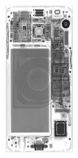
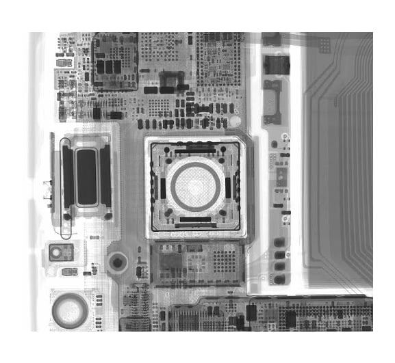
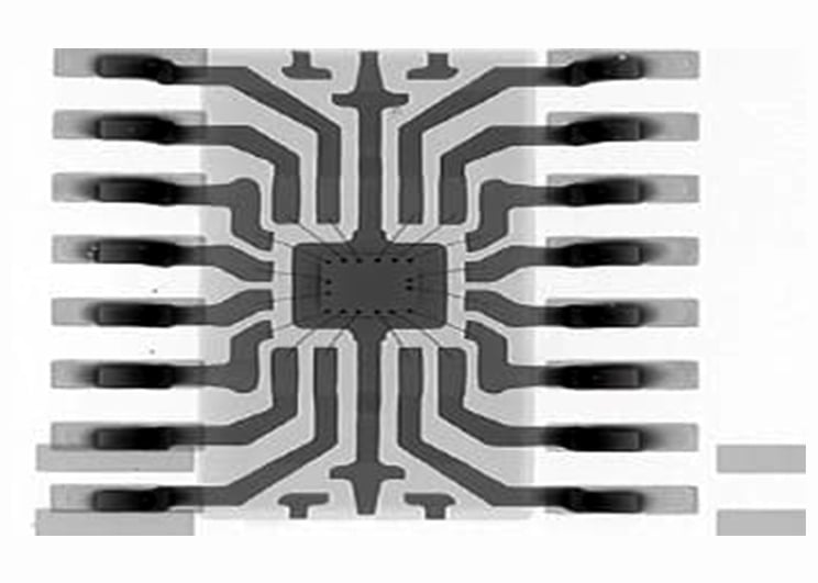
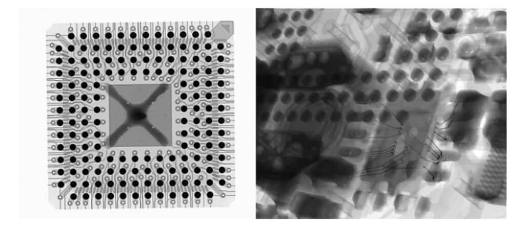
Sample Requirements
- Requires solid samples or samples that can be glued in place to limit vibrations.
- Samples need to be stable under normal atmospheric conditions.
- Samples need to be a maximum size of 740 x 580 mm (29 x 22.8 inches).
- Samples are limited to a maximum weight of 5 kg (11lbs).
- The inspection area can be up to 510 x 445mm.
2D X-Ray Inspection Applications by Industry
Electronics & Semiconductor
Detects solder voids, cracked balls, bridging, lifted wires, and Head in Pillow defects in BGA.
Battery & Energy Storage
Reveals voids, cracks, or delamination in electrodes and seals.
Medical Devices & Biomedical
Ensures proper assembly of miniature implantable devices.
General Materials Science General Materials Science
Identifies inclusions, porosity, and fractures in composites and metals.
PCBA Inspection Services
Identify via misalignment, shorts, and layer defects in complex boards.
Techniques That Complement 2D X-Ray Inspection
Why Choose Covalent for Your 2D X-Ray Imaging Needs?
Covalent offers industry-leading expertise in 2D X-ray inspection, delivering rapid results for PCB and BGA X-ray inspections. Our team tailors X-ray metrology conditions for each project, ensuring reliable detection of solder voids, interconnect failures, and subtle assembly defects.
Whether you need fast PCBA inspection services or in-depth non-destructive failure analysis, our solutions provide clarity and actionable insight.