
Nanoindentation testing presses a diamond tip into the surface with forces as low as a few micronewtons and continuously records load versus depth. That curve reveals hardness, elastic modulus, stiffness, creep, and viscoelastic behavior, without the substrate effects that limit conventional hardness tests on thin films and coatings.
What Is a Nanoindentation Test?
A nanoindentation test presses a precisely shaped diamond tip into a material and records the applied force and penetration depth throughout loading and unloading. Analyzing that load–displacement curve gives hardness, elastic modulus, and how the material deforms. Because loads and depths are tiny, nanoindentation can measure thin films, coatings, and site-specific regions on devices and components with micron-scale lateral precision.
High-Resolution Mechanical Testing
Measures hardness and modulus of thin coatings and small features.
Dynamic Analysis Capability
SINUS-mode loading measures storage and loss modulus for viscoelastic materials.
Temperature-Dependent Profiling
Measures mechanical properties from room temperature to about 200 °C.
Why Use Nanoindentation?
Nanoindentation delivers elastic modulus, hardness, creep, stiffness, yield-related behavior, and storage and loss modulus from a single test platform. Fracture toughness (K_IC) can be estimated by measuring indent-induced cracks with SEM or optical microscopy.
Compared with conventional microhardness methods such as Vickers or Brinell, nanoindentation uses far smaller loads and depths, so it can measure a thin coating without the substrate skewing the result.
Material Compatibility
Plastics, metals, ceramics, coatings, and thin films. Very soft materials such as hydrogels and some biopolymers are more challenging.
Resolution / Measurement Scale
Depth resolution of about 0.01 nm and load resolution of about 1 µN, with micron-range lateral stage accuracy.
Depth Profiling
SINUS or progressive multi-cycle loading shows how properties change with depth.
How Nanoindentation Works
Every test follows the same sequence, with dynamic and heated options added when you need them.
- Approach and contact. A diamond tip, usually a three-sided Berkovich indenter, approaches and contacts the surface. Covalent's reference indenter keeps surface contact stable, even during long measurements on soft or time-dependent materials.
- Load, hold, and unload. Force rises to a set maximum, holds briefly to capture creep, then releases. Load and depth are recorded continuously throughout.
- Analysis. Hardness is calculated from the maximum load and the contact area. Elastic modulus comes from the slope of the unloading curve, using the Oliver–Pharr method.
- Dynamic and temperature options. In SINUS mode, a small oscillating load is added to measure stiffness and storage and loss modulus continuously with depth. A heated stage extends measurements from room temperature to about 200 °C.

Nanoindentation for Thin Films and Coatings
Thin films are where nanoindentation is most valuable, and where test design matters most.
- The 10% rule: keep indent depth below about 10% of the film thickness so the substrate does not influence the hardness result. Modulus is more sensitive, so very thin films may need shallower indents or modeling.
- Depth profiling: SINUS or progressive multi-cycle loading shows how hardness and modulus change with depth, separating the film's response from the substrate's.
- Film vs. film-plus-substrate: our scientists choose loads and depths based on your film thickness and roughness, and report whether results reflect the film alone or the composite system.
- Adhesion and wear: pair indentation with nano scratch testing to measure coating adhesion, delamination loads, and scratch resistance.
For broader programs, see our coating testing services.
Equipment Used for Nanoindentation

Anton Paar STeP (Standard Testing Platform) 600
The Anton Paar STeP 600 platform at Covalent includes three testing heads:
UNHT3 — Ultra Nanoindentation Tester
- Supports sinusoidal loading for dynamic mechanical testing.
- Includes a temperature-controlled sample stage from room temperature to approximately 200 °C for hardness, modulus, and viscoelastic measurements versus temperature.
MCT3 — Micro-Combi Tester
Used for micro-indentation and micro-scratch measurements.
NST3 — Nano-Scratch Tester
Used for nanoscale scratch and coating-response measurements.
Key Differentiators
Key capabilities include SINUS-mode dynamic mechanical testing and a reference-indenter approach that helps maintain reliable surface contact during long-duration measurements or testing of relatively soft/time-dependent materials.
Strengths
- Small force and displacement resolution for thin coatings and small features.
- Room-temperature to 200 °C property profiling.
- Dynamic mechanical testing for viscoelastic materials.
Limitations
- Concave sample surfaces are generally not ideal and might require additional sample preparation prior to testing.
- Features at or below roughly 5 µm can be difficult to measure accurately depending on geometry and setup.
- Very soft materials may require alternate approaches or partner-lab capabilities.
- High surface roughness can increase measurement variability.
Example Outputs
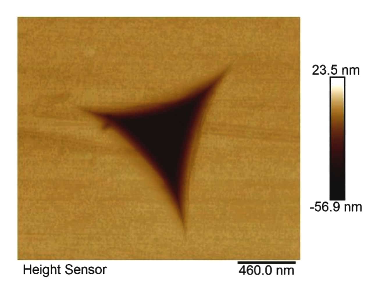
AFM imaging can be used to inspect indents in reference materials such as fused quartz and to support verification of contact geometry or calibration.
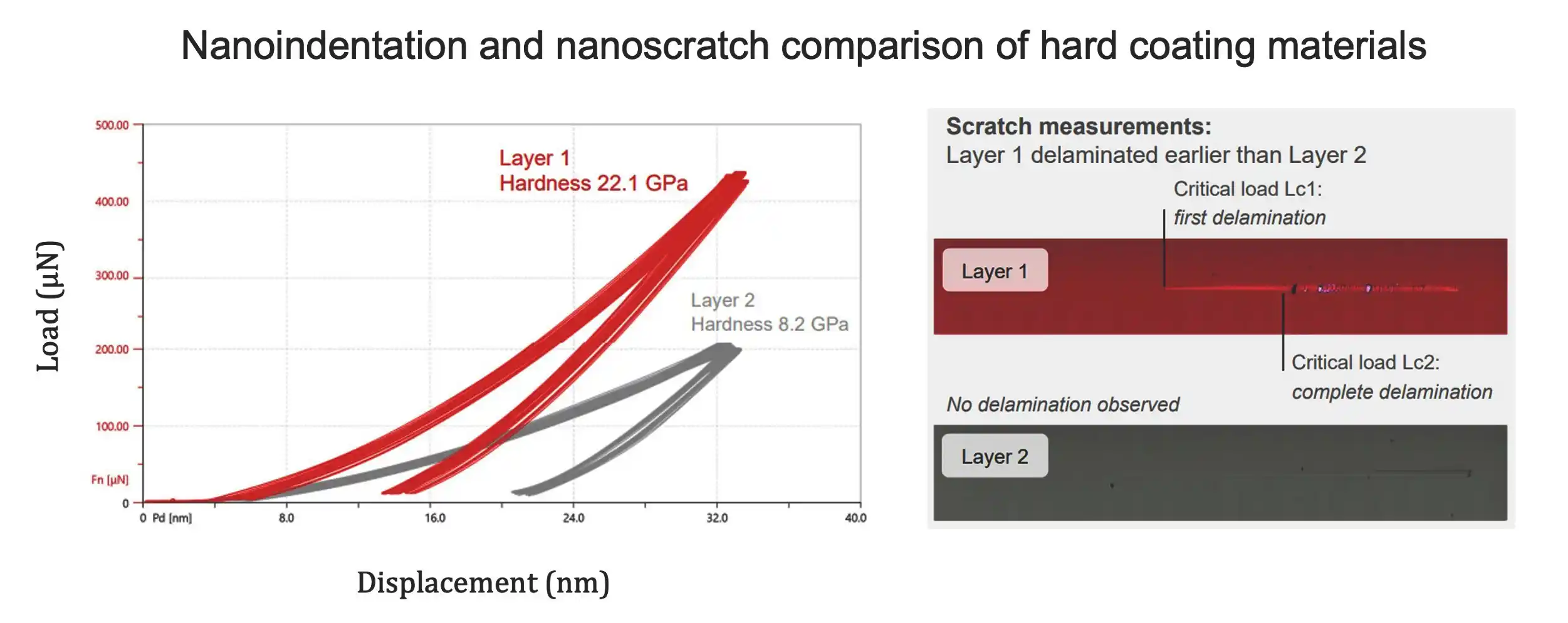
Indentation and progressive-load scratch tests can compare coating systems; differences in penetration under the same load can indicate differences in hardness or resistance to deformation.
Sample Requirements
Samples should be solid and preferably flat. Non-flat samples may require mechanical preparation. Surface roughness may also need to be characterized so that an appropriate load and penetration depth can be selected.
Nanoindentation Applications by Industry
Semiconductor
Mechanical-property measurements on low-k dielectric and other thin-film structures.
Battery
Hardness measurements on isolated graphite or other electrode particles.
Consumer Electronics
Localized measurements on small device features and layered structures, including advanced logic-device materials.
Medical
Temperature-dependent storage/loss modulus measurements of pressure-sensitive adhesives used in sensors and other devices.
Techniques That Complement Nanoindentation
Techniques such as ICP-OES, SEM-EDS, or GD-OES can be used to correlate film chemistry with measured mechanical properties.
Progressive-load scratch testing can characterize shear, delamination, and coating adhesion behavior and can be compared with hardness data.
Microscopy can document indent morphology and cracks. For fracture-toughness-related analysis, crack lengths extending from indent edges may be measured.
Why Choose Covalent for Your Nanoindent Needs?
Covalent performs nanoindentation using the Anton Paar STeP 600 platform with UNHT3 dynamic/SINUS capability and a temperature-controlled stage. The reference-indenter configuration supports stable contact during time-dependent measurements, and live collaboration during setup can help tailor loads, locations, and outputs to the application.
Frequently Asked Questions
What properties can Nanoindent measure?
Common outputs include hardness, elastic modulus, creep response, stiffness, yield-related behavior, fracture-related response, and dynamic storage/loss modulus.
What types of materials can be tested?
Metals, ceramics, plastics, coatings, and thin films are common candidates.
What are the spatial and depth resolutions?
Depth resolution is approximately 0.01 nm, load resolution is approximately 1 µN.
What complementary techniques are useful?
Optical microscopy or SEM can visualize indents and cracks, while scratch testing can evaluate coating adhesion, shear, and delamination behavior.
Can mechanical properties be measured at elevated temperature?
Yes. The UNHT3 setup includes a heating stage for measurements from room temperature to approximately 200 °C.