
What Is Raman Spectroscopy?
Raman spectroscopy analyzes the inelastic scattering of monochromatic light, usually from a laser, to identify molecular vibrations and gain insight into a substance’s structure and composition. Raman scattering occurs when incident photons interact with molecular or lattice vibrations within the sample, causing a shift in energy that results in scattered light with different wavelengths, either higher (anti-Stokes) or lower (Stokes) than the incident light. Each material exhibits a unique Raman spectrum, enabling reliable identification and characterization based on its molecular structure and composition.
Enhanced Sensitivity Options
High Spatial and Depth Resolution
Versatile Sample Compatibility
Why Use Raman Spectroscopy?
Raman spectroscopy can be used to map or identify the structure & chemistry of samples at the sub-micron scale. The Raman signal is often used to identify the type and nature of chemical compounds by comparing the sample signature against reference standards.
Unique Chemical Fingerprinting
Non-Destructive High-Precision Analysis
Wide Industry Applications
Supports analysis in semiconductors, pharmaceuticals, polymers, and advanced materials research.
How Raman Spectroscopy Works
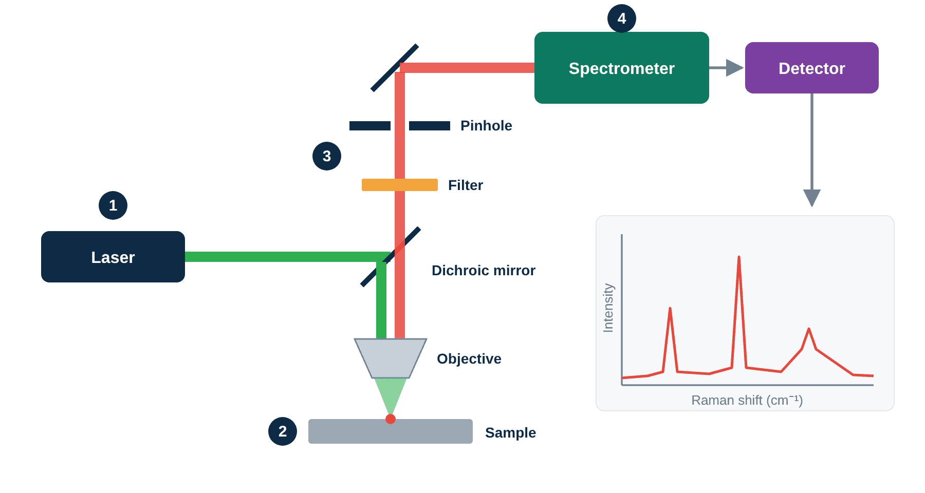
1. Excite the sample. A laser of a single wavelength is focused onto the sample through a microscope objective. Covalent offers 355, 455, 532 and 785 nm, so the wavelength can be matched to the material and kept away from fluorescence.
2. Scatter the light. Most of the light bounces back at the same wavelength (Rayleigh scattering). About one photon in ten million exchanges energy with the sample’s molecular bonds or crystal lattice and comes back shifted in wavelength. This is the Raman signal, and the size of the shift is a fingerprint of the chemical bonds and crystal structure.
3. Filter and focus. A filter removes the much stronger laser light, and a confocal pinhole passes only light from the focal spot. This lets us analyze features about a micron across, or a single layer within a stack, without signal from the material around it.
4. Read the spectrum. A spectrometer spreads the light by wavelength onto a detector, producing a spectrum of intensity against Raman shift (cm⁻¹). Peak positions identify the material, peak shifts reveal stress and strain, and peak widths indicate crystallinity. Scanning the laser point by point builds chemical and stress maps, up to full 300 mm wafers.
Equipment Used for Raman Spectroscopy
Our Raman and photoluminescence spectroscopy capabilities span multiple instrument platforms, allowing us to tailor laser excitation wavelength, confocal optics, and measurement conditions to each sample and application. We also integrate Raman spectroscopy with complementary analytical techniques to deliver a more complete understanding of a sample’s composition, structure, defects, and material properties.

Oxford Instruments WITec360 Semiconductor Edition
- Confocal Raman and photoluminescence (PL) microscope designed for advanced materials and semiconductor characterization
- Excitation sources:
- 355 nm.
- 532 nm.
- 300 mm wafer capability: Motorized vacuum wafer stage supports automated mapping and characterization of semiconductor wafers up to 300 mm in diameter.
- TrueSurface™ Topography tracking: Maintains optimal focus across rough, curved, patterned, and non-planar samples by automatically following surface topography.
- Vibration-isolated platform: enables high stability measurements.
- Configurable spectral resolution: Multiple spectrometer grating options can support both wide spectral range acquisitions and high-resolution characterization.

ThermoFisher Scientific DXR3xi Raman Spectrometer
- Multiple Excitation Lasers:
- 455 nm.
- 532 nm.
- 785 nm.
- Laser Power with precision controls: 0.1 mW power increments.
- Spatial Resolution: Better than 0.5 micron.
- Confocal Depth Resolution: Better than 2 micron.
- Maximum image area: 101.6 mm x 76.2 mm.
Key Differentiators
- Excitation in the UV, VIS, and NIR for various sample types.
- Micron and sub-micro scale information can be obtained.
- Topography-aware measurements – TrueSurface™ tracking maintains focus across patterned and non-planar semiconductor structures.
- Surface enhanced Raman scattering (SERS) can provide enhanced sensitivity for certain compounds.
Strengths
- Non-destructive.
- Can measure samples through glass and other transparent containers.
- Works for most samples, liquids, gases or solids.
- Confocal microscopy provides depth resolution (~1-2um) for non-destructive depth profiling of layered.
Limitations
- Laser confocal microscope configuration probes a small spot/volume, around 1um, which requires multiple spots to adequately sample heterogeneous materials. Fast mapping of many particles or locations can be beneficial.
- Most metals are difficult/impossible to measure.
- Highly fluorescent samples can overwhelm the weaker Raman signal, in certain cases higher or lower excitation wavelengths can overcome this.
- Certain vibrational modes are forbidden due to sample symmetry.
Example Outputs
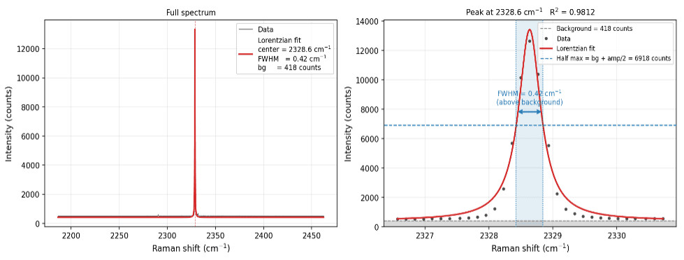
Raman spectrum of liquid nitrogen demonstrating the high spectral resolution of the WITec 360 Raman microscope. A Gaussian fit to the Raman peak yields a linewidth of 0.42 cm-1, highlighting the system’s ability to resolve closely spaced spectral features and detect subtle peak shifts.
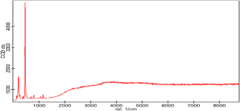
UV Raman spectrum of crystalline quartz. The characteristic Si–O vibrational mode near 464 cm⁻¹ is clearly resolved with a high signal-to-noise ratio. With UV excitation, Raman and the photoluminescence features are well-separated, minimizing interference within the Raman fingerprint region and improving confidence in peak identification.
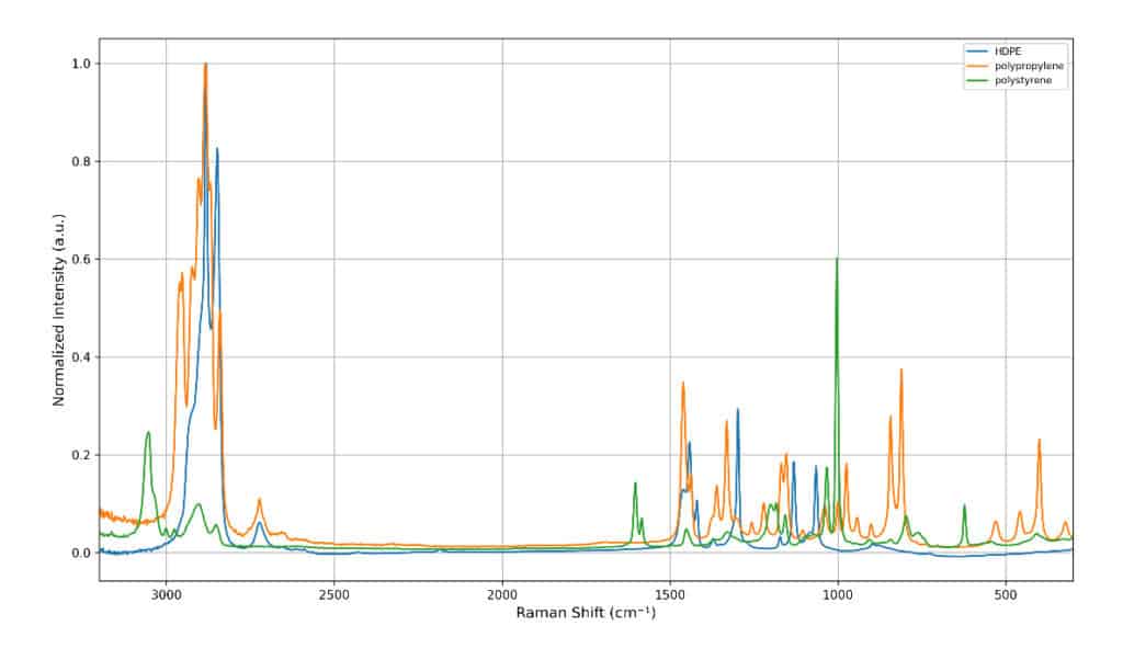
Comparison of Raman spectra for polystyrene, polypropylene, and high-density polyethylene, illustrating distinct peak patterns that enable clear discrimination and identification of these polymers.
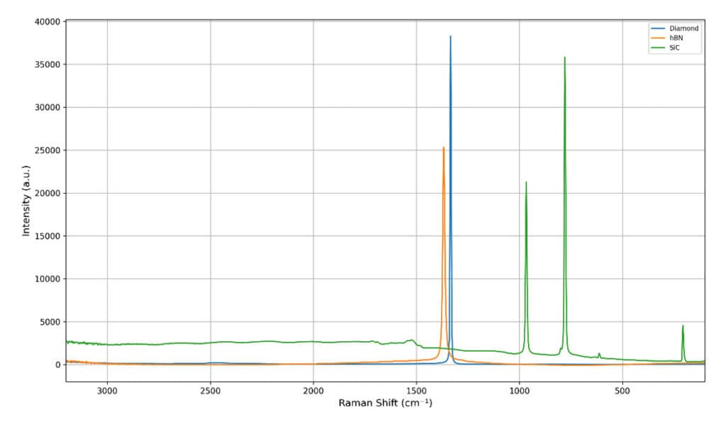
Raman spectra of boron nitride, silicon carbide, and diamond highlighting the distinct strong phonon peaks characteristic of each material.
Sample Requirements
- Solids, powders, films, fibers, particles and liquids can all be measured, mostly as received, in air with no vacuum or coating.
- Feature size: down to about 1 µm. Wafers: up to 300 mm.
- Samples must tolerate laser exposure. Sensitive or dark materials are run at reduced power.
- Highly fluorescent samples may need a different laser wavelength (355, 455, 532 or 785 nm).
- Pure metals give little or no Raman signal, but oxides and coatings on metals can be measured.
Raman Spectroscopy Applications by Industry
Analysis of Graphite Quality
Raman spectroscopy evaluates graphite crystallinity and defect density by examining the intensity and shape of the D, G, and 2D bands. In addition to quality different polymorphs (nanotubes, graphene, C60, diamond, etc.) can be easily distinguished.
Strain Mapping in Semiconductors
Raman shifts of phonon modes are sensitive to strain and provide a non-destructive way to detect and quantify strain/stress in semiconductor wafers and devices. Using the mapping capabilities strain gradients at the microscale can be characterized.
Mapping Active Ingredients in Pharmaceuticals
Raman imaging allows spatially resolved identification and distribution of active pharmaceutical ingredients (APIs) and excipients within tablets and other solid formulations. Often used to QA/QC in pharmaceutical manufacturing. Different crystal polymorphs can also be distinguished.
Polymer Identification
Raman spectroscopy enables identification of polymer materials by comparison to an extensive reference library. This is well suited for small particles, thin layers and localized contamination where FTIR is not practical. Raman can also measure particles behind transparent materials like glass as it relies on visible or NIR light.
Battery Development
Identifying active materials, monitoring structural and chemical changes from cycling, and mapping compositional variations across electrodes and solid electrolytes. Supporting materials research, quality control, and failure analysis.
Photonics & Quantum Materials
Crystal quality assessment, stress characterization, phase identification, and structural characterization of optical materials, wide-bandgap semiconductors, integrated photonic devices, and quantum materials.
2D Materials
Layer number determination, crystal quality assessment, strain and doping analysis, phase identification, and spatial mapping of transition metal dichalcogenides (TMDs) and van der Waals heterostructures.
Minerals and Geology
Rapid, nondestructive identification of minerals, phases, and polymorphs based on their characteristic vibrational signatures. Spatially resolved measurements support mineral mapping, inclusion analysis, contamination identification, and characterization of geological materials with micron-scale spatial resolution.
Techniques That Complement Raman Spectroscopy
Raman Spectroscopy Testing Services at Covalent
Covalent combines advanced confocal Raman microscopy with a broad portfolio of materials characterization and failure analysis capabilities. Our Raman spectroscopy platforms offer multiple excitation wavelengths, configurable spectral resolution, and high-spatial-resolution mapping, allowing measurements to be optimized for a wide range of materials and analytical challenges.
Beyond collecting Raman spectra, we help customers understand the underlying causes of observed material behavior. Raman results can be integrated with our in-house spectroscopy, profilometry, SEM, XPS, FIB, TEM, XRD, and other analytical techniques to accelerate root-cause investigations, process optimization, product development, and materials research.