
What is PL Spectroscopy?
Photoluminescence (PL) spectroscopy is a non-destructive optical characterization technique that probes the electronic structure of materials by measuring the wavelength and intensity of light emitted following laser excitation at a specified wavelength. The resulting emission spectrum provides insights into the material properties. Configured with the geometry of a confocal microscope, PL microscopy enables high-resolution mapping of these properties to assess material uniformity.
Why use PL Spectroscopy?
Photoluminescence (PL) analysis provides a rapid, non-destructive way to evaluate material quality and uniformity. Analyzing PL spectra can reveal information about optical emission characteristics, defects, impurities, and recombination behavior that can impact device performance. Confocal PL microscopy enables high-resolution mapping of the uniformity of these properties along a sample, across a wafer, and through the depth below transparent surfaces.
- Multiple laser options – Available excitation wavelengths across near-UV, visible, and near-IR
- Sample mapping – across 300mm wafers or small, high-resolution areas
- Broad material compatibility – semiconductors, 2D materials, perovskites, and quantum materials.
Identify process-induced changes
Map wafer non-uniformity
Enable targeted root-cause analysis
How Photoluminescence (PL) Spectroscopy Technique Works
Photoluminescence (PL) spectroscopy measures the light emitted from a material after it is excited with a laser. Different excitation wavelengths can be used to optimize the measurement for specific material systems and optical transitions. The absorbed energy promotes electrons to higher-energy states, and as these electrons relax and recombine, they emit photons with characteristic wavelengths. In a confocal microscope geometry, the emitted light is collected with high spatial resolution, enabling localized analysis of material quality, optical properties, defects, strain, and recombination behavior.
Equipment Used for PL
Our photoluminescence and Raman spectroscopy capabilities span multiple instrument platforms, allowing us to tailor laser excitation wavelength, confocal optics, and measurement conditions to each sample and application. We also integrate these spectroscopy studies with complementary analytical techniques to deliver a more complete understanding of a sample’s composition, structure, defects, and material properties.
Equipment for Photoluminescence (PL) Spectroscopy

Oxford Instruments WITec360 Semiconductor Edition
- Confocal Raman and photoluminescence (PL) microscope designed for advanced materials and semiconductor characterization
- Excitation sources:
- 355 nm.
- 532 nm.
- 300 mm wafer capability: Motorized vacuum wafer stage supports automated mapping and characterization of semiconductor wafers up to 300 mm in diameter.
- TrueSurface™ Topography tracking: Maintains optimal focus across rough, curved, patterned, and non-planar samples by automatically following surface topography.
- Vibration-isolated platform: enables high stability measurements.
- Configurable spectral resolution: Multiple spectrometer grating options can support both wide spectral range acquisitions and high-resolution characterization.

ThermoFisher Scientific DXR3xi Raman Spectrometer
- Multiple Excitation Lasers:
- 455 nm.
- 532 nm.
- 785 nm.
- Laser Power with precision controls: 0.1 mW power increments.
- Spatial Resolution: Better than 0.5 micron.
- Confocal Depth Resolution: Better than 2 micron.
- Maximum image area: 101.6 mm x 76.2 mm.
Key Differentiators
- Excitation in the UV, VIS, and NIR for various sample types.
- Micron scale information can be obtained.
- Topography-aware measurements – TrueSurface™ tracking maintains focus across patterned and non-planar semiconductor structures.
- Integrated analytical workflows – PL results can guide targeted SEM, FIB, TEM, SIMS, XPS, and other follow-on analyses.
Strengths
- Non-destructive characterization.
- Can measure samples through glass and other transparent containers.
- Confocal microscopy provides depth resolution for non-destructive depth profiling into semi-transparent surfaces.
Limitations
- Laser confocal microscope configuration probes a small spot/volume, around 1um, which requires multiple spots to adequately sample heterogeneous materials. Fast mapping of many particles or locations can be beneficial.
- For materials with strong absorption at the laser wavelength, this technique may only probe the surface.
- PL spectroscopy can reveal the presence and distribution of defects, but complimentary techniques will be needed to determine their exact composition or structure.
Example Outputs
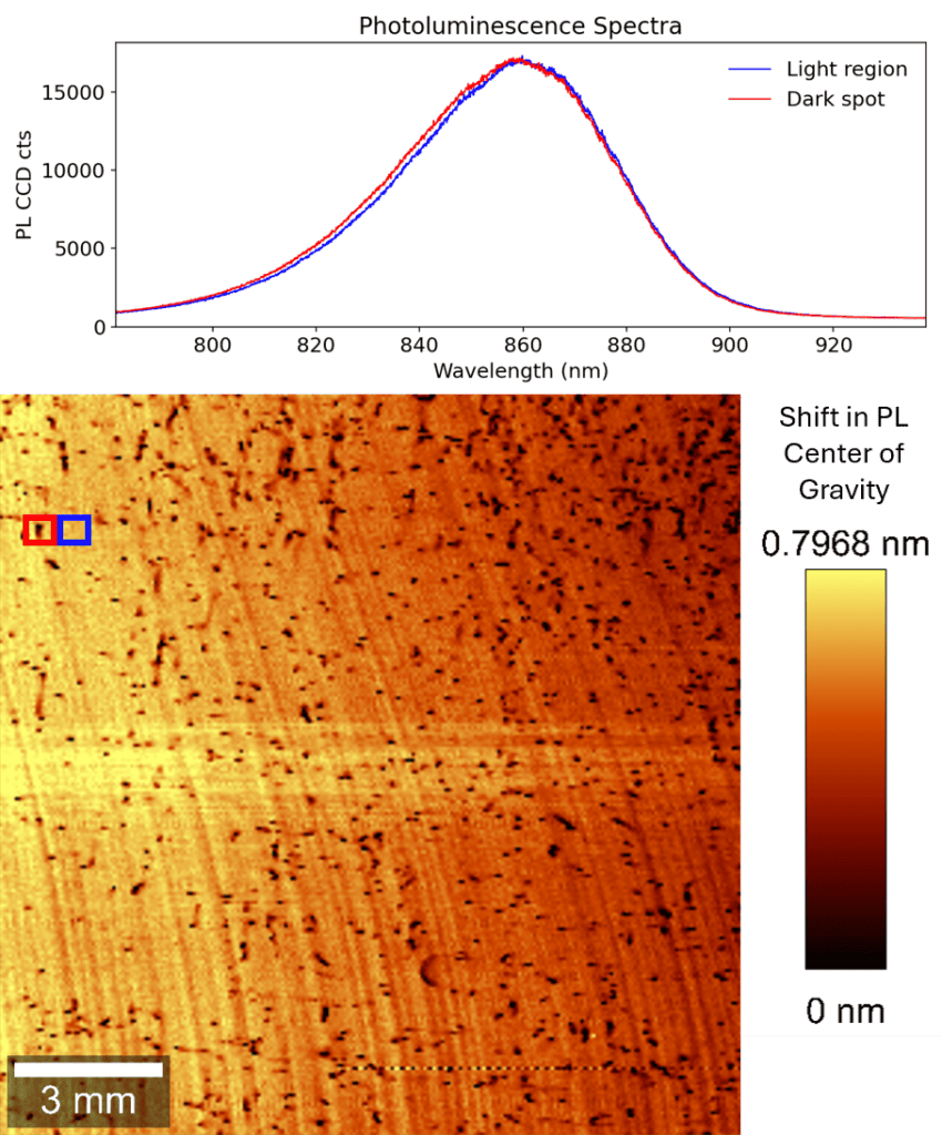
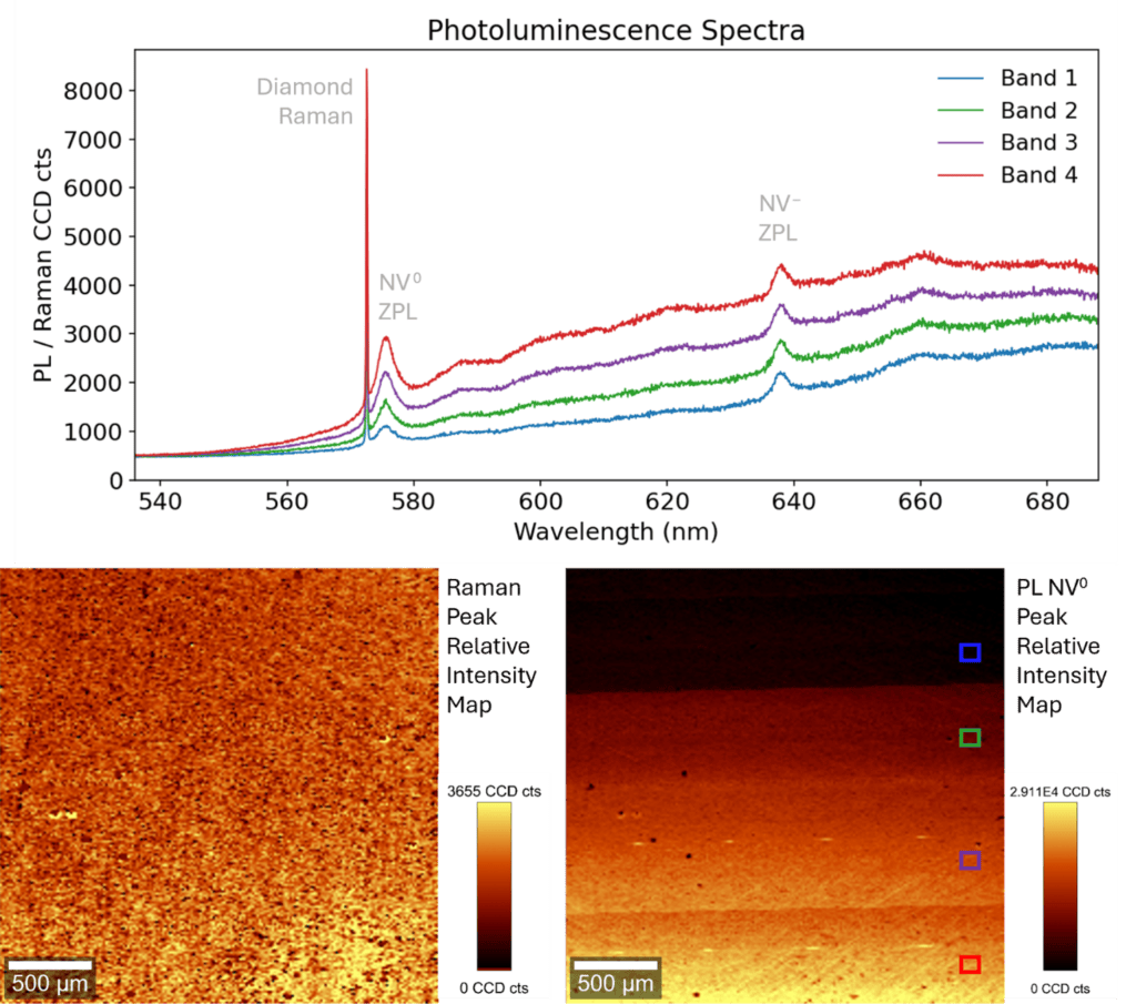
Depending on the project, outputs can include raw emission spectra, tables of emission band peak position and intensity, and 1D or 2D scans.
Sample Requirements
Sample must be stable under laser irradiation; reduced power can be used to mitigate. Strongly absorbing samples can be sensitive.
Photoluminescence (PL) Spectroscopy applications by industry
Semiconductor
Defect mapping, wafer uniformity assessment, epitaxial layer thickness, doping concentrations, process-induced damage evaluation, strain analysis, and failure analysis.
Power Electronics
Defect characterization in SiC and GaN devices, material quality assessment, process optimization, thermal characterization under electrical bias, failure analysis and reliability investigations.
Solar Cells
2D Materials
Photonics & Optoelectronics
Techniques That Complement PL
Performed on the same instrument platform, Raman spectroscopy complements PL by providing information on material identification, crystal phase, stress/strain, crystallinity, and molecular bonding.
Provide complementary molecular identification and chemical bonding information, particularly for polymers, organics, and other infrared-active materials.
Reveals crystal defects, dislocations, interfaces, and atomic-scale structure responsible for observed photoluminescence characteristics.
Why Choose Covalent for Your Photoluminescence Spectroscopy Needs?
Covalent combines advanced photoluminescence instrumentation with a broad portfolio of materials characterization and failure analysis services. Our confocal PL/Raman spectroscopy platforms support multiple excitation wavelengths and configurable spectral acquisition, enabling measurements to be tailored to your specific application.
Additionally, Covalent helps customers understand the underlying cause of observed behavior. PL results can be integrated with our in-house spectroscopy, profilometry, SEM, XPS, FIB, TEM, and other analytical techniques to accelerate root-cause investigations, process optimization, and materials development efforts.