
What Is X-ray reflectometry (XRR)?
X-ray reflectometry is a non-destructive X-ray characterization technique that is used to understand top layer film thicknesses, densities and interfacial roughness of film stacks whose approximate chemistries and thicknesses are known.
XRR is able to characterize a wide range of measurable film types, such as metallic, dielectric and transparent films.
Layer Stack Analysis
Non-Destructive Measurement
High Sensitivity & Precision
Why Use XRR?
- High-Level Advantages (e.g., non-destructive testing and high sensitivity).
- XRR allows for characterization of the properties of the top layer stacks of a material.
Use XRR instead of TEM when the sample cannot be altered/destroyed. XRR is non-destructive in nature and does not take the intensive sample preparation needed for TEM analysis.
Advanced Instrumentation
Versatile Sample Handling
Optimized Scans and Modeling
How X-ray Reflectometry Analysis Works
In X-ray reflectometry (XRR analysis) an X-Ray source supplies a high-brilliance beam of X-rays which reflect off a flat surface at very low incident angles.
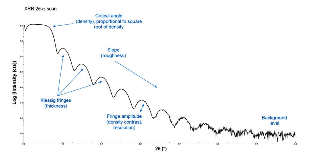
The XRR system then measures the intensity of the X-rays reflected in the specular direction (where the reflected angle is equal to the incident angle). If the interface between layers or between a layer and the substrate is not perfectly sharp and smooth, the reflected intensity will deviate from that predicted by the law of Fresnel reflectivity.
The deviations of the X-ray reflectometry can then be analyzed to obtain the density profile of the interface normal to the surface and modeling can be used to determine layer thicknesses, densities, and interfacial roughnesses.
Equipment Used for XRR

Rigaku XTRAIA MF-3000
- Covalent has a 9kW rotating anode Rigaku SmartLab that allows for higher energy X-rays than other labs.
- The Rigaku XTRAIA MF-3000 has both XRR and EDXRF capabilities allowing elemental analysis as well as thickness, density, and roughness information on the same location on a wafer as well as wafer mapping.
Key Differentiators
- XRR is beneficial for semiconductor industries.
- Within the semiconductor industry, XRR allows for better understanding of film growth and deposition.
Strengths
- XRR is an invaluable tool for better understanding the top layers of materials. It is a non-destructive way of understanding the thickness, density and roughness of film stacks.
- XRR is also able to characterize a wide range of measurable film types, such as metallic, dielectric and transparent films.
- XRR’s non-destructive nature allows for samples to be characterized and returned for future processing which may not be possible using other methods.
Limitations
- The chemistry of the material and approximate film thicknesses is necessary to perform XRR modeling. A completely unknown sample is unable to be identified using XRR. It is recommended that a chemical or elemental technique be coupled with XRR for full comprehension of a material.
- XRR samples usually require flat, uniform sample surfaces with a roughness of less than 2nm for accurate results.
- Lateral inhomogeneities cannot be incorporated into XRR models.
- XRR has a longer scan time than that of SE.
- XRR is limited to films less than 100s nm, which TEM is not restricted to.
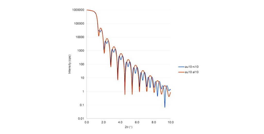
Example Outputs
Sample Requirements
- Samples must be solid.
- Samples must be smooth, uniform, flat, with a roughness of less than 2nm and film thickness from ~1nm to 100s of nm.
- Sample wafers must be eight inches or smaller for the in-house Rigau SmartLab.
- Sample wafers for the Rigaku XTRAIA MF-3000 can range up to 300mm.
X-ray Reflectometry Applications by Industry
Semiconductor Manufacturing
Measures thin film thickness, density, and roughness during wafer fabrication to improve process control and device performance.
Thin Film Process Development
Provides precise, non-destructive feedback on new deposition recipes and multilayer stack designs
Photonic & Optical Coatings
Validates dielectric and reflective coatings where nanometer level thickness and interface quality directly affect optical performance.
Nanostructured Materials
Analyzes ultrathin films, superlattices, and 2D materials with high resolution, enabling non-destructive assessment of complex nanoscale structures.
Techniques That Complement XRR
- Any technique with chemical or elemental analysis is a great complement for XRR. XRR cannot determine the chemical makeup of a sample. XRR is often paired with techniques such as EDXRF / WDXRF, SEM/EDS, FTIR, or even XPS.
- Complementary techniques to further confirm film thickness and other properties are SE and TEM.
- Using the Rigaku XTRAIA MF-3000, both XRR and EDXRF characterization is possible, allowing elemental analysis as well as thickness, density, and roughness information on a wafer.
Why Choose Covalent for Your XRR Needs?
Covalent tailors each XRR scan to the sample and applies advanced modeling to resolve complex film stacks with confidence. Using the Rigaku XTRAIA MF-3000, we can combine XRR measurements of thickness, roughness, and density with EDXRF chemical analysis at the same sample locations. This integrated approach enables detailed wafer mapping and provides a more comprehensive understanding of thin film composition and structure.