
What Is Cathodoluminescence (CL)?
Cathodoluminescence (CL) occurs when a material gives off light after being hit with an electron beam. It is often used together with a scanning electron microscope (SEM), which allows researchers not only see the structure but also to understand the deeper properties of a sample. CL goes beyond just the elemental makeup; it can reveal band gaps, crystalline defects, impurities, and carrier concentrations with impressive detail.
With resolution down to about 100 nm, SEM imaging confirms exactly where the signal is coming from. CL can also create 2D maps of material properties, and by adjusting the electron beam, scientists can control how deep the analysis goes. Covering a wide wavelength range from 200 to 1600 nm, it’s a versatile and powerful way to study what’s really happening inside advanced materials.
Crystalline Insight
Non-Destructive Mapping
High Spatial Resolution
Why Use CL?
Cathodoluminescence (CL) is a non-destructive and highly sensitive technique that can be used in place of photoluminescence (PL) when information from a much smaller volume at the nanometer scale is required. It is particularly valuable for analyzing crystalline defects and is widely applied in fields such as semiconductors, including LSIs, ICs, and discrete devices, as well as in power electronics and optoelectronic components like LEDs, laser diodes (LDs), and photodiodes (PDs).
Defect Sensitivity
Depth‑Tunable Analysis
SEM‑Correlated Mapping
How Cathodoluminescence Measurement Works
When a specimen is irradiated with an electron beam, various types of electrons are emitted, including characteristic X-rays. Light in the ultraviolet, visible, and near-infrared regions is called Cathodoluminescence (CL). CL is generated through the process of:
- Generation of carriers (electron-hole pairs).
- Carrier diffusion.
- Radiative recombination.
Characteristic X-rays have element information. On the other hand, CL reflects information about crystallinity and stress.
Equipment Used for CL

JEOL JSM-7100F/TTLS
Improved with Horiba’s specially ordered original high-speed and sensitive UV-VIS-NIR CL system.
Specifications:
- The detectable wavelength is from 200 to 1600 nanometer, which corresponds to ultraviolet, visible, and near-infrared regions.
- Acceleration voltage: 0.5~30kV.
- Beam current: ~300nA.
- Measurement area: 2mm2~500nm2.
- Sample size: Less than 10 x10 mm2.
Key Differentiators
CL is a unique technique that provides electron microscopy and spectroscopic analysis, Our CL system has the following two main features.
- Nanometer-level surface analysis using a low-energy, high-current electron gun.
- High-speed, high-sensitivity spectral mapping using cutting-edge software.
Strengths
- CL is a powerful technique to characterize crystalline defects in materials. Scanning electron microscope (SEM) images can be used to identify the target location of the specimen. It is a great advantage of CL from the viewpoint of spatial resolution. The detection depth can be easily tuned by changing the electron beam energy.
- Plan-view CL with several nm detection depth is practically useful for the failure analysis of semiconductor devices because the devices have a multilayered thin film structure. Moreover, the CL has a high affinity to other electron-beam-based technologies like energy dispersive X-ray spectrometry (EDX) and electron beam induced current (EBIC).
Limitations
- Materials susceptible to electron beam damage (e.g. organic materials, biological materials) are not well-suited.
Example Outputs
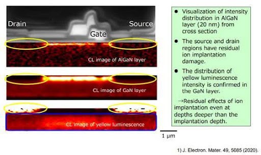
- Characterization of ion implantation damage for AIGaN in HEMT device: We analyze gallium nitride high-electron-mobility transistor devices, which are crucial for high-speed communications, from a cross-sectional perspective. The thickness of the aluminum gallium nitride layer is about 20 nanometers. However, we can clearly observe the luminescence from the thin aluminum gallium nitride layer. In the source and drain regions, high-dose ions are implanted, and the intensity is reduced due to the ion implantation damage. Furthermore, as to the yellow luminescence, which originates from the point defects in gallium nitride, we can see that the intensity becomes weak in the lower part of the source and drain regions. In general, the implanted ions do not reach such a deep region. Residual effects of ion implantation are observed even at depths deeper than the implantation depth.
- Spectral mapping measurements can be used for device process optimization, failure analysis, and reverse engineering of the products.
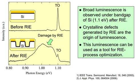
- RIE process optimization by the evaluation of crystalline defects in Si: Despite the extensive investigation of new semiconductors like SiC and GaN, Si is still the most important semiconductor. CL has advantages in the analysis of Si-based devices because:
- A Si wafer is a nearly perfect crystal. The defects are often generated during device fabrication.
- SEM can be used for the identification of measurement points. The relevant area in the devices can be easily identified.
- Depth-resolved measurement can be easily achieved by changing the acceleration voltage.
Sample Requirements
- Physical form: Solid.
- Necessary properties: Stable in vacuum.
- There is no minimum sample size.
- Preparation or constraints depend on the contents that the customers need.
CL Applications by Industry
Semiconductor
CL makes invisible damage visible. From spotting ion implantation issues in AlGaN HEMTs to tracking crystalline defects in silicon during RIE, it helps optimize processes and boost device reliability.
Techniques That Complement Cathodoluminescence
Why Choose Covalent for Your Cathodoluminescence Needs?
Our services are designed to find details about your materials that other techniques cannot reach. Whether you are working with semiconductors, power devices, or advanced optical materials, CL gives you a better understanding and look at crystal defects, imperfections, and nanoscale structures, without harming your sample.