
What Is Scanning Electron Microscopy?
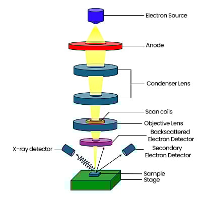
Scanning electron microscopy (SEM) is an analytical technique that produces an image of a sample and other signals by scanning the surface with a high energy beam of electrons. The electron beam interacts with the atoms of the sample to produce many different signals that contain detailed information including the surface topography and chemical composition of the sample.
Flexible Sample Handling
Analyzes diverse solid samples, including thin films, powders, and bulk materials, with conductive preparation options.
Comprehensive Analysis Mode
Supports topography, elemental composition, crystallography, and 3D reconstruction with advanced detectors.
Ultra-High Resolution Imaging
Resolves features below 1 nm with excellent depth of field for 3D-like surface views.
Why Use SEM?
Our SEM analysis delivers critical insights that accelerate research and development while enhancing quality control through high-resolution imaging to detect and resolve material issues. For time-sensitive projects, Covalent offers rapid turnaround with expedited processing to provide results in as little as 24 hours. Every project is supported with comprehensive reporting, including detailed documentation of measurement conditions and results, ensuring clear and actionable insights. This data empowers informed decision-making, guiding strategic choices in product development and manufacturing processes.
Accelerated Research and Development
Delivers nanoscale insights that drive innovation and material optimization.
Improved Quality Control
Identifies defects, contaminants, and compositional issues to enhance product reliability.
Rapid and Actionable Results
Provides high-quality imaging and elemental analysis with fast turnaround times.
How SEM Works
SEM provides the user with the ability to see and capture images of the morphology of sample surfaces to visually identify key features and areas of interest.
Equipment Used for SEM

Thermo Scientific Helios 5 UC DualBeam FIB‑SEM
- Electron column: Elstar Extreme high-resolution field-emission SEM column with Magnetic immersion lens.
- Electron beam: Accelerating voltage 350 V–30 kV; resolution 0.6 nm at 15–30 kV and 0.7 nm at 1 kV.
- Source: High-stability Schottky FEG delivering ~0.8 pA–100 nA probe current.
- Detectors: In-lens SE/BSE (TLD), ETD SE, optional in-column SE/BSE/MD, DBS, and retractable STEM 3+ BF/DF/HAADF.
- Stage: High-precision 5-axis motorized stage (up to 150 × 150 mm XY).
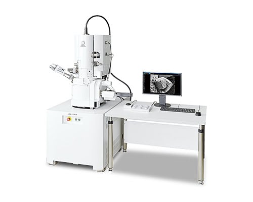
JEOL JSM‑IT800HL Schottky FEG SEM
- Electron gun: In-lens Schottky Plus field-emission gun with probe currents up to 300 nA at 30 kV.
- Electron beam: Landing voltage 0.01–30 kV; resolution 0.7 nm at 20 kV and 1.3 nm at 1 kV.
- Objective: Hybrid Lens for versatile high-resolution imaging.
- Detectors: Standard SED and UED; optional SBED and segmented VBED for compositional and topographic contrast.
- Stage: Full eucentric 5-axis motorized goniometer stage (up to 170 mm-diameter samples).
Key Differentiators
- EDS on multiple tools.
- EBSD on Helios 5 UC.
- Low vacuum/environmental mode on Scios.
- Multiple tools with ultra-high resolution (UHR) immersion final objective lens.
- Electrostatic final objective lens for magnetic materials on Scios.
- Air free transfer module compatible with JEOL IT-800HL.
- 150mm X-Y stage range.
- 3D reconstruction capability with Thermo Fisher Slice and View feature and Aviso software.
Strengths
- High spatial resolution.
- Excellent surface topography and depth of field.
- Wide range of magnification.
- Ability to perform elemental/compositional analysis.
- Multiple imaging modes, flexible sample size and geometry.
- Rapid imaging capabilities.
Limitations
- Samples analyzed with SEM are done under a high vacuum environment and therefore must be vacuum stable.
- Liquids or volatile outgassing materials are not compatible with SEM.
- Magnetic materials can be analyzed with appropriate caution.
- Magnetic samples in ultra-high-resolution mode are avoided to avoid damaging the instrument.
Example Outputs
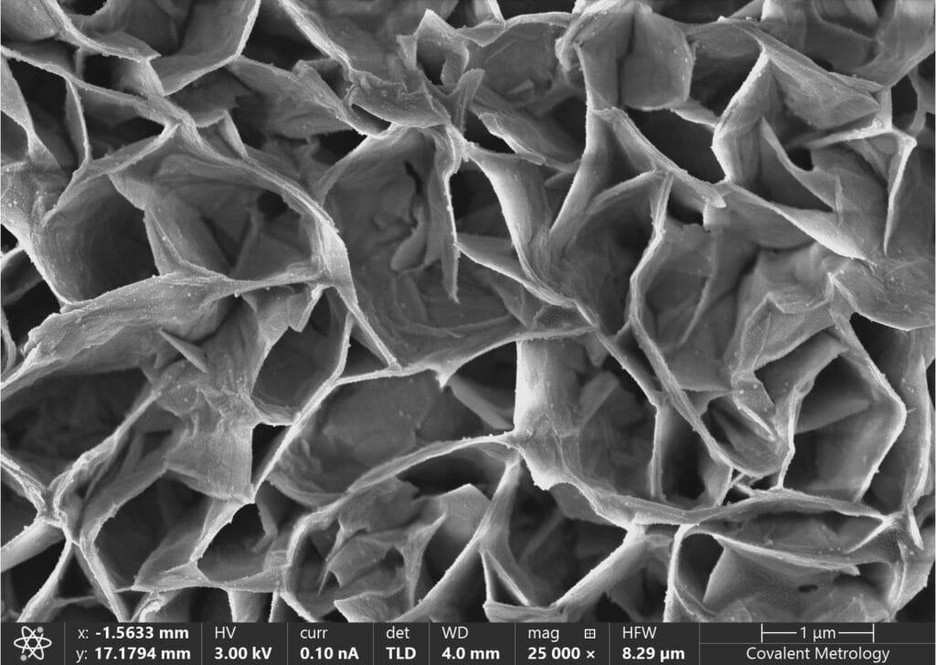
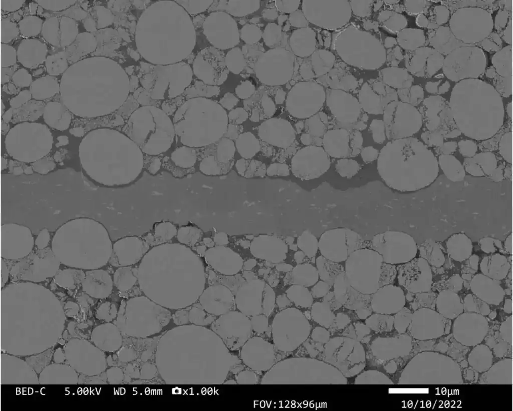
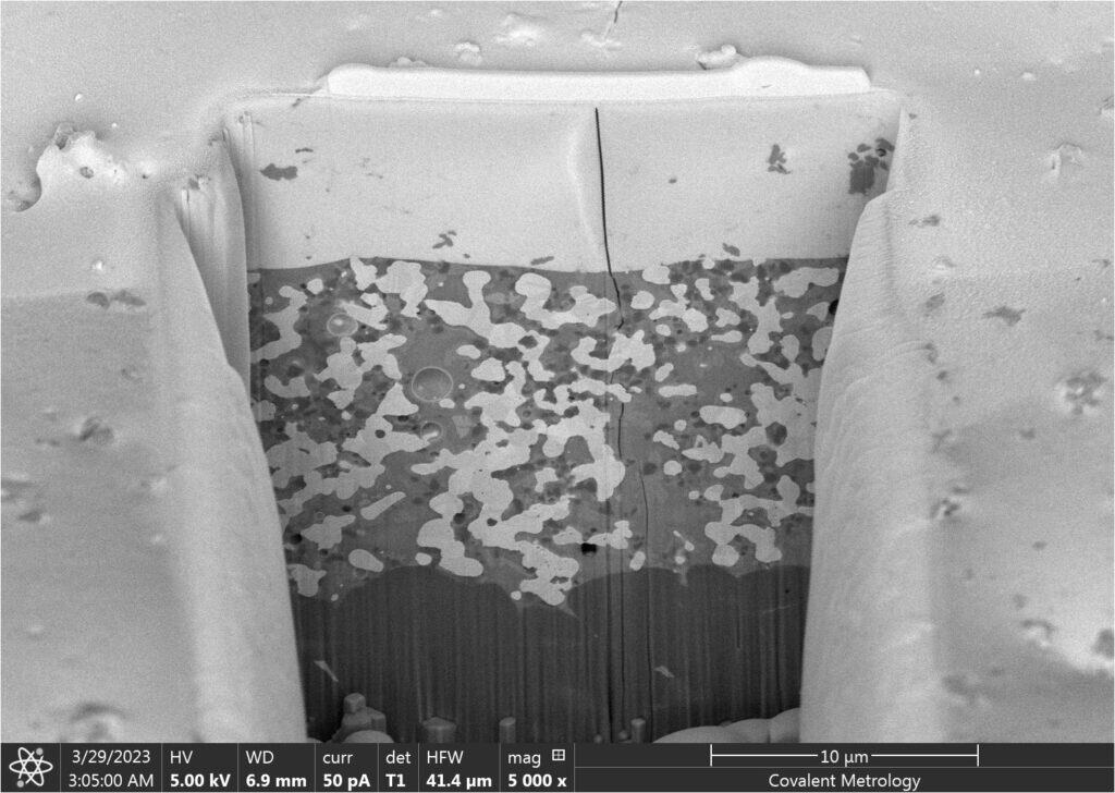
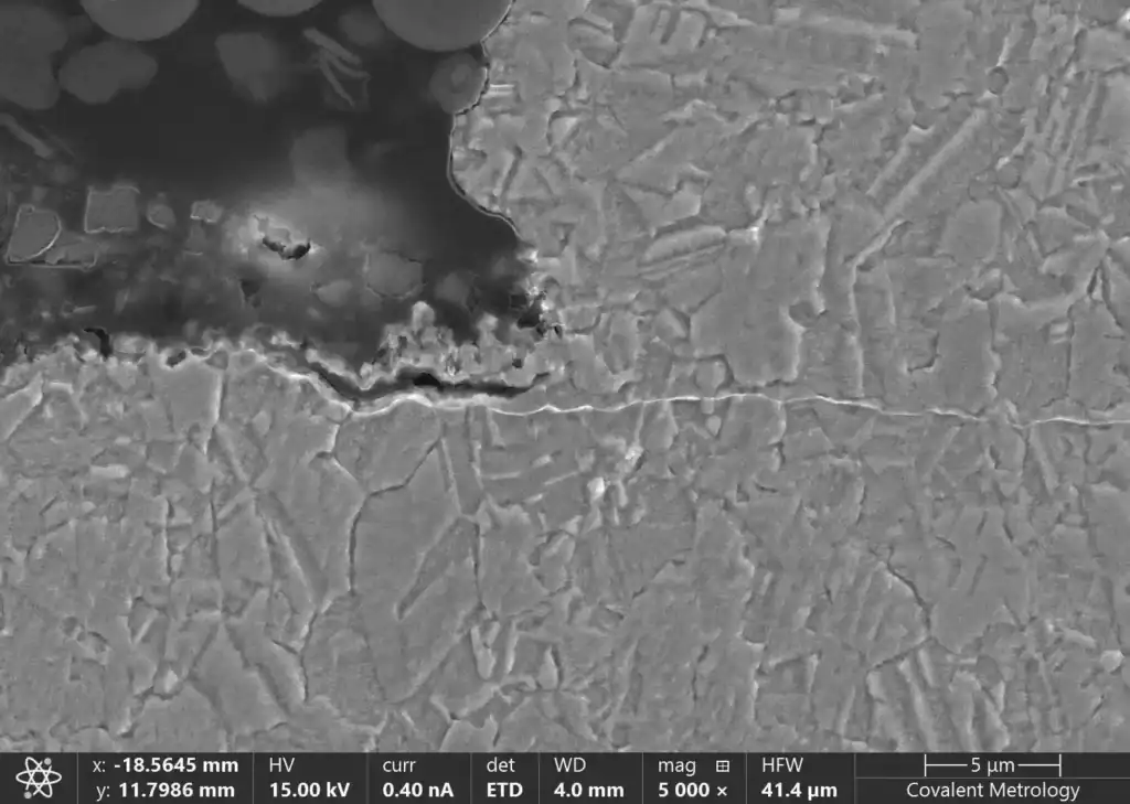
Typical SEM output is greyscale images with differences in contrast depending on the type of detector. A data bar is also found on the image and usually contains info on the accelerating voltage, SEM detector type, beam current, stage tilt, working distance, magnification, horizontal field width and a scale bar.
- SE greyscale contrast describes surface topography including brighter contrast at edges and high spots, and darker contrast for regions of shadow, valleys and holes. Good for highlighting different morphologies such as cracks, fibers and textures.
- BSE greyscale contrast describes composition contrast. Heavier elements with higher Z appear brighter, and lighter elements with lower Z appear darker. Can be used to determine compositional differences and locate different phases or materials.
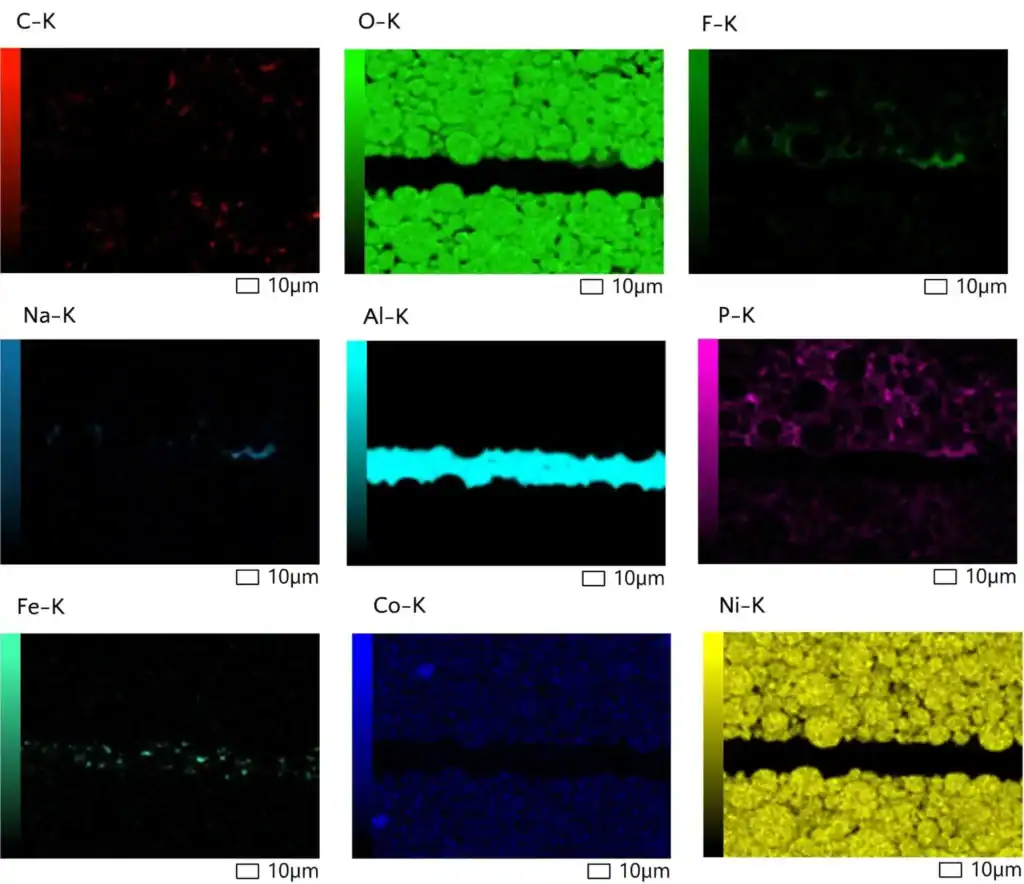
- EDS output of data typically involves X-ray spectra, elemental maps or linescans.
- X-ray spectra are graphs that display X-ray energy on the X axis, and X-ray counts on the Y axis. The peaks in the spectra are matched to the specific X-ray energies of elements and used to determine the chemical composition of the area of interest (weight percent or atomic percent).
- Elemental maps visually display where in an area of interest specific elements are found. The brightness of the map in a specific area corresponds with how highly concentrated the element is in the AOI. The maps are color coded by element and can be overlaid on top of the SEM image.
- EDS linescans measure the X-ray EDS data along a single line. The data output is a line graph displaying X-ray count intensity vs position along the line. The different elements are color coded and can be overlaid with each other. The Y axis can be converted to weight percent or atomic percent.
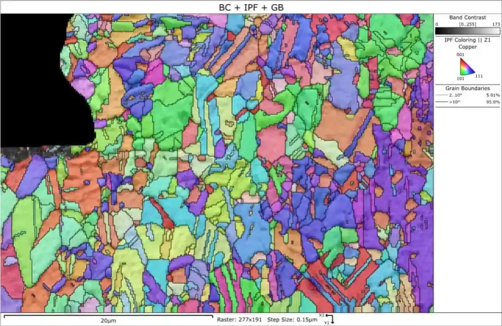
- EBSD outputs include grain orientation maps, phase identification maps, grain size distribution charts, grain boundary maps.
- Grain orientation maps are color coded such that certain colors correspond to the crystallographic orientation of a sample grain for a specific crystal system.
If multiple material phases are being measured simultaneously, phase maps provide color coded display of the locations of the different phases in the field of view.
Sample Requirements
- Solid state samples required including thin films on substrates, powder samples, bulk samples.
- Must be vacuum compatible, no outgassing, volatile samples.
- Electrically conductive samples. Non-conductive samples will require additional preparation to apply a conductive coating.
- Samples should be thermally and mechanically stable under vacuum conditions and beam exposure. Need to be mounted to the stage or aluminum stubs with conductive tape or other adhesives.
- Samples need to be large enough to be easily manipulated with physical tools such as tweezers or powder scoops.
- Minimum detectable concentration with EDS is 0.1 atomic percent.
- Samples with significant variations in height may not be compatible especially for SEMs that have a short optimal working distance. This is especially true when FIB milling is also required.
- Samples requiring FIB milling should generally be flat and the area of interest on the top most surface of the sample. Some exceptions can be made depending on the geometry of the sample.
- Sample size, shape and weight are important considerations for sample mounting and orientation for SEM analysis and FIB milling. Samples need to be mechanically stable and not drift while the stage is tilted during FIB milling. Specialized sample holders and fixtures may be required for complex samples.
SEM Applications by Industry
Aerospace
- Wear, corrosion, and fatigue analysis.
- Characterization of composite interfaces.
- Grain structure and boundary visualization.
Automotive
- Fractography (failure analysis).
- Surface defects in 3D‑printed parts.
- Coating thickness and uniformity.
Metallurgy
- Surface morphology of metals.
- Grain structure and boundary visualization.
- Texture, phase identification, strain and deformation studies using EBSD.
Semiconductor Fabrication
- IC defect inspection and failure analysis.
- Lithography pattern verification.
- Surface contamination or damage inspection.
- Thin film stack analysis using FIB‑SEM‑EDS.
Consumer Electronics
- Surface contamination or damage inspection.
- Identification of unknown contaminants using SEM‑EDS, often coupled with FTIR.
Medical Devices
- Wear, corrosion, and fatigue analysis.
- Characterization of composite interfaces.
- Coating thickness and uniformity.
Pharmaceuticals
- Analysis of mixed powder samples using FIB-SEM-EDS to investigate cross sections, particle shape and size, and layered structure.
- Identification of unknown contaminants on samples using SEM-EDS and FTIR.
Li‑ion Battery Manufacturing
- Analysis of mixed powder samples using FIB‑SEM‑EDS to investigate cross sections, particle shape and size, and layered structure.
- Identification of unknown contaminants on samples using SEM‑EDS and FTIR.
Techniques That Complement SEM
SEM Testing Services at Covalent
Our clients trust Covalent Metrology for SEM analysis results that exceed their expectations. We provide industry-leading, high-resolution scanning electron microscopy capabilities that offer superior data essential for understanding and optimizing the quality of your materials.
Frequently Asked Questions
What is SEM used for?
An SEM uses a focused beam of electrons to scan the surface of a sample, generating high-resolution images that reveal surface topography, composition, and sometimes crystallography at micro- to nanoscale. Its high resolution and depth of field make it invaluable across many disciplines.
How do you interpret SEM images?
Interpretation of SEM images relies on understanding how different contrast mechanisms relate to sample features, beam settings, and detector types. For topographic contrast using secondary electrons, bright areas are regions of the sample that are facing the detector, whereas dark areas are recessed or shadowed. This allows one to identify cracks, voids, fibers, rough surface, and 3D surface shapes. For compositional contrast using backscattered electrons, bright areas are higher atomic number elements and darker areas are lower atomic number elements (gold vs carbon). This type of contrast allows one to identify inclusions, multi-phase materials, contamination, and coating layers.
What are the advantages of SEM?
The advantages of Scanning Electron Microscopy (SEM) are:
- Nanometer resolution: Visualize fine surface details.
- High depth of field: Capture complex 3D surfaces in focus.
- Multipurpose detectors: Topography, composition, crystallography.
- Wide sample compatibility: Hard, soft, conductive, non-conductive materials.
- Elemental microanalysis: Map and quantify elements at the microscale.
- In situ and correlative tools: Study processes in real time; integrate with other techniques.
- Fast and reproducible imaging: Efficient data collection and analysis.
What is FIB-SEM and how does it work for material analysis?
Focused bean scanning electron microscopy (FIB-SEM) analysis allows for site-specific, nanoscale sample preparation for both surface and subsurface analysis by using a focused ion beam for high precision material removal for in-situ sample modification for high resolution imagings before and after material removal.
What are the best practices for preparing samples for SEM-EDS and FIB-SEM analysis?
For SEM-EDS and FIB-SEM, samples should be clean and free of dust or oils to avoid imaging artifacts and interference with elemental analysis. Non-conductive materials often require a thin conductive coating, while small or irregular samples should be securely mounted for stability in the vacuum.