
FIB-SEM analysis combines a focused ion beam, which mills material away with nanometer precision, and a scanning electron microscope, which images the exposed surface. It is used to cut site-specific cross-sections, prepare TEM lamellae, and build 3D reconstructions of subsurface features in devices, coatings, batteries, and other materials.
What Is Focused Ion Beam Scanning Electron Microscopy?
Focused ion beam scanning electron microscopy (FIB-SEM) uses two beams in one instrument. The ion beam removes material to expose subsurface features, and the electron beam images them at high resolution. Combined with EDS, it reveals the chemical composition of specific regions. FIB-SEM works on metals, ceramics, polymers, and semiconductors, with lateral milling resolution of about 5–10 nm using a Ga⁺ ion beam, and it reaches from nanometers to tens of microns below the surface.
Composition
Combined with EDS, maps elemental composition alongside structural detail.
Versatility
Compatible with metals, ceramics, polymers, and semiconductors, accommodating diverse research and industrial needs.
Resolution
Captures nanoscale detail of subsurface features for precise structural analysis.
Why Use FIB-SEM?
FIB-SEM is the go-to tool for precise, site-specific analysis of micron- and submicron-scale features in devices, thin films, composites, and other materials. It exposes the exact location you need, extracts and thins lamellae to electron transparency (about 100 nm) for transmission electron microscopy (TEM), and builds 3D reconstructions at nanometer resolution. Imaging and milling happen in one system, with correlative SEM, EDS, and EBSD on the same cut face.
Precision
Targets specific regions of interest with nanometer-level accuracy.
Versatility
Supports metals, semiconductors, ceramics, polymers, and bio-samples across multiple imaging modes.
3D Insight
Enables FIB-SEM tomography for volumetric understanding of nanoscale structure.
How FIB-SEM Works
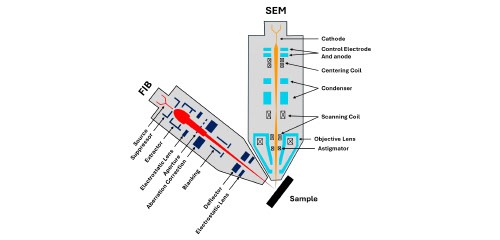
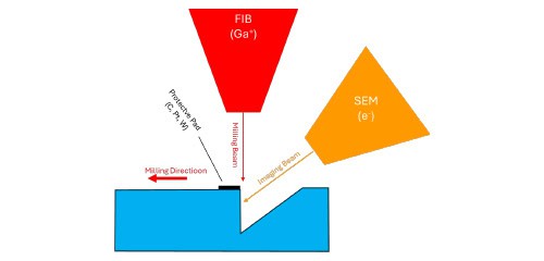
A FIB-SEM, also called a dual-beam system, positions an electron column and an ion column at an angle so both beams meet at the same point on the sample. A typical analysis follows four steps:
- Locate the feature. The SEM images the surface to find the defect, layer, or region of interest.
- Protect the surface. A thin platinum layer is deposited over the site to preserve the top surface during milling.
- Mill. The ion beam removes material to cut a trench, a cross-section, or a lamella, usually with the stage tilted to 52°.
- Image and analyze. The SEM images the exposed face, with EDS for composition and EBSD for crystal orientation.
Milling can range from nanometers to tens of microns. Gallium and plasma ion sources behave differently; read Gallium vs. Plasma FIB: What's Actually Happening Inside the Column for the trade-offs.
FIB-SEM Services
Three new sections, each targeting a search people make for a specific FIB service.
FIB Cross-Sectioning
FIB cross-sectioning exposes a precise vertical face through a defect, layer stack, solder joint, or interface, without the smearing or delamination that mechanical polishing can cause. A protective platinum cap preserves the top surface, and the cut face is imaged with SEM and mapped with EDS. Cross-sections can reach up to about 100 µm wide and tens of microns deep.
What you get: SE and BSE images of the cross-section, layer thickness measurements, EDS maps, and EBSD on request.
TEM Lamella Preparation
Covalent prepares site-specific TEM lamellae from wafers, devices, and bulk materials, thinned to electron transparency (under about 100 nm). Automated AutoTEM software delivers fast, repeatable lamella preparation, and low-kV final polishing reduces surface damage. Lamellae go straight to our TEM and STEM for imaging, EDS, and EELS. Learn more in our webinar Preparing Better TEM Samples Faster.
What you get: a site-specific lamella, preparation images showing its location, and optional TEM or STEM analysis.
FIB-SEM Tomography (Slice and View)
FIB-SEM tomography mills away thin slices and images each new face to build a 3D reconstruction of the volume. It reveals the size, shape, connectivity, and distribution of pores, particles, cracks, and phases that a single cross-section can miss, for example in battery electrodes, catalysts, and porous films. Reconstructions use Thermo Fisher Slice and View with Avizo software.
What you get: the image stack, 3D renderings, and quantified volume fractions and pore or particle statistics.
Equipment Used for FIB-SEM

ThermoFisher Scientific Helios 5 UC Dual Beam
- Electron beam resolution:
- At optimum WD:
- 0.6 nm at 30 kV STEM.
- 0.7 nm at 1 kV.
- 1.0 nm at 500 V (ICD).
- At coincident point:
- 0.6 nm at 15 kV.
- 1.2 nm at 1 kV.
- At optimum WD:
- UC+ monochromator.
- Ion Optics: Down to 500kV for final polishing on TEM lamella.
- Automated TEM Prep for fast/repeatable throughput: Thermo Scientific™ AutoTEM™ Software for automated STEM sample preparation.
- Sample:
- Max sample weight: 500 g (including sample holder).
- Max sample size: 150 mm with full rotation (larger samples possible with limited rotation).

ThermoFisher Scientific Helios 6 HD Dual Beam
- New FIB column with automated source and column alignments provides increased stability and low-kV milling capabilities.
- New digital scanning and patterning engine allows for simultaneous SEM imaging and FIB milling which enables more precise end-pointing and higher productivity.
- AutoTEM 6 Software-targeted application designed to deliver the most out of the new Helios 6 HD FIB-SEM’s hardware platform. This AI-enabled software automatically aligns all grid/finger locations, offering enhanced grid management capabilities and a decrease in set-up time.
- Longer interval between EasyLift NanoManipulator needle exchanges and streamlined replacement, leading to increased system availability and consistent results.
Key Differentiators
Strengths
- Fine details in surface topography, such as texture, roughness, and microstructure, are easy to see.
- Able to view the shape, size, and arrangement of particles, fibers, pores, grains, etc., due to the high magnification range and depth of field.
- Can provide precise 2D measurements of lengths, diameters, feature sizes, such as layer thicknesses, pore or particle sizes.
- Qualitative or semi-quantitative chemical composition of visible features.
Limitations
- SEM needs vacuum-stable, conductive samples.
- Magnetic materials can be analyzed with caution, using field-free observation modes. Avoid ultra-high resolution mode.
- FIB milling is incompatible with low vacuum modes.
- Spatial resolution is worse than TEM and degrades with high voltage/light elements.
Example Outputs
Sample Requirements
- Solid phase.
- Must be vacuum stable.
- Maximum Sample Height: 55 mm.
- Maximum Sample Weight: 500 g (including sample-holder).
- Maximum Lateral Dimension: 150 mm (larger samples enabled with reduced rotation).
FIB-SEM Applications by Industry
Semiconductor
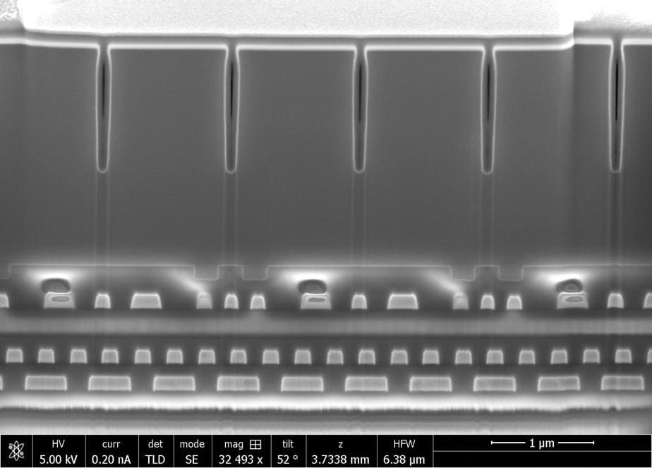
FIB-SEM is often used for failure analysis and process monitoring on semiconductor samples. The FIB can be used to make cross sections on the nanoscale while SEM is used in combination with EDS to image and chemically characterize the cross section.
Materials
FIB cross-section of copper foils for EBSD analysis of the cross-section for grain size and crystallographic orientation analysis.
Battery Technology
Recurring Covalent client requires routine sample analysis of a thin film stack. Covalent has successfully optimized the FIB-SEM-EDS procedures for these samples to minimize turnaround time and deliver quality data to the client.
TEM Lamella Prep
For multiple industries, including semiconductor fabrication, semiconductor devices, data storage, IC packaging, battery, optoelectronics, coatings/thin films, life sciences, and medical devices.
Techniques That Complement FIB-SEM
FIB-SEM Testing Services at Covalent
Our clients trust Covalent for SEM analysis results that exceed their expectations. We provide industry-leading, high-resolution scanning electron microscopy capabilities that offer superior data essential for understanding and optimizing the quality of your materials.