
What Is Digital Optical Microscopy?
Digital optical microscopy uses advanced optical microscopes to generate images like modern digital cameras, capturing the light reflected from or transmitted through a sample under set illumination. However, unlike a simple camera, modern optical microscopes also include intrinsic lens systems and sophisticated illumination systems that facilitate high magnification and dynamic range images with micron-scale resolution. Applications include imaging and measuring critical dimensions, defect features, solder connections, and cross-sectioned parts in the semiconductor, materials science, and precision manufacturing industries.
Analytical Support
Advanced Imaging
Performance
Why Use Digital Optical Microscopy?
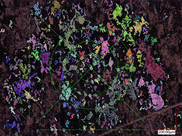
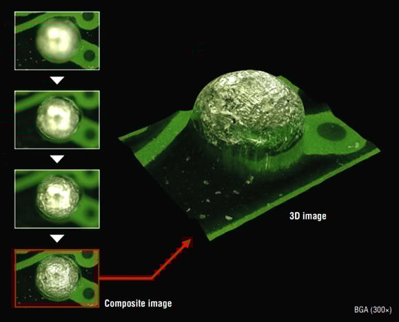
Our 3D optical microscopy services use extended depth-of-field optics with automated compositing and image stitching to integrate images captured across multiple focal planes and large areas. This produces fully focused, high-resolution images across the entire field of view, even with significant height variations. A high-precision automation system provides precise control over different illumination modes for optimal imaging quality.
Versatile Illumination
Depth-of-Field Imaging
Large-Area Image Stitching
How Digital Optical Microscopy Works
Digital Optical Microscopy captures high-resolution images using advanced lenses and controlled illumination. Automated depth-of-field compositing and image stitching generate entirely focused images on complex surfaces. Adjustable lighting and tilting ensure precise edge definition and accurate dimension measurements.
Equipment Used for Digital Optical Microscopy

Keyence VHX-X1
- Dynamic Microscope Tilt Range: -89° to +89° from vertical.
- Magnification Range: 20x to 6000x.
- Maximum Field of View 15.24 mm (lateral) x 11.40 mm (vertical) at 20x magnification.
- Illumination Modes: customizable bright-field, dark-field, and mixed lighting.
- High-precision, automated, in-situ dimensional analysis.
- High-quality depth composition imaging.

Keyence VHX-6000
- Dynamic Microscope Tilt Range: −60° to 90° from vertical.
- Magnification Range: 20× to 2000×.
- Maximum Field of View: 15.24 mm (lateral) × 11.40 mm (vertical) at 20×.
- Illumination Modes: Customizable bright‑field, dark‑field, and mixed lighting.
- Capabilities: High‑precision, automated, in‑situ dimensional analysis.
Key Differentiators
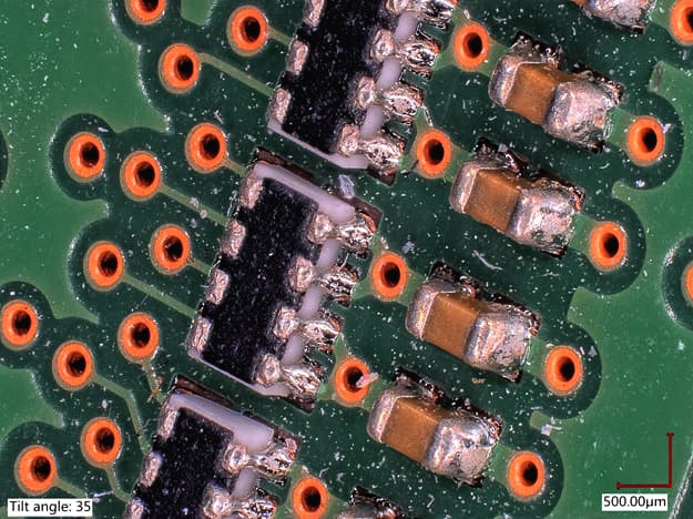
Our optical microscopy systems can tilt the microscope relative to the sample and image with a high depth of field to enhance edge definition and improve feature visibility on complex geometries.
Strengths
- High-resolution and accurate imaging.
- Reproducible images with multi‑modal illumination and extended depth of field.
- Widest possible depth-of-field (without cross-sectioning) among direct imaging/microscopy techniques.
Limitations
- It does not have as high a spatial resolution as other scanning probe microscopy methods, such as AFM.
- It may be less efficient when more precise 3D-height measurements are needed.
- Covalent’s other techniques may be a better fit in certain cases.
Example Outputs
Sample Requirements
We accept solid and liquid samples (liquids must be in sealed containers). The maximum sample mass is 5 kg. The maximum solid dimensions are 100 mm (L) × 100 mm (W) × 40 mm (T). For larger parts, we can separate and/or cross‑section components to expose the features of interest.
Digital Optical Microscopy Applications by Industry
Semiconductor & Electronics
Digital optical microscopy is used to inspect ICs, wafers, PCBs, and advanced packaging for defects, delamination, and grain structure. It enables non-destructive failure analysis, precise surface imaging, and dimensional verification of microfeatures.
Materials & Manufacturing
Supports dimensional inspection, surface quality assessment, and defect detection in machined or fabricated parts. Ideal for verifying tolerances and identifying imperfections in precision components.
Mechanical Testing & Research
Used to examine crack propagation, indentation patterns, and deformation zones after mechanical or thermal stress testing, offering visual correlation with material behavior.
Polymers & Coatings
Captures surface texture, layer uniformity, and microstructural defects in coatings, thin films, and polymer components to ensure quality and consistency during processing.
Medical Devices & Packaging
Evaluates bonding, sealing, and surface finish in medical assemblies and packaging, ensuring integrity and compliance under strict manufacturing standards.
Techniques That Complement Digital Optical Microscopy
Why Choose Covalent for Your Digital Optical Microscopy Needs?
Optical microscopy is fast, affordable, and effective, but at Covalent, it’s elevated through advanced digital systems and a broad suite of complementary tools. Our experts combine optical, confocal, WLI, SEM, and AFM methods to deliver focused, high-resolution views and actionable measurements for defect, dimensional, and microstructure analysis. For urgent or complex projects, we offer rapid turnarounds and live, guided sessions with our engineers.