
X-ray photoelectron spectroscopy (XPS), also called ESCA, shines X-rays on a sample and measures the energy of the electrons that escape from its top 7–10 nm. Those energies identify every element except hydrogen and helium and show each one's chemical state, such as metal or oxide. XPS is widely used to study surface contamination, oxidation, and thin-film chemistry.
What Is X-ray Photoelectron Spectroscopy?
X-ray photoelectron spectroscopy (XPS), also known as electron spectroscopy for chemical analysis (ESCA), is a surface-sensitive technique that probes the top 70–100 Å (7–10 nm) of a sample. X-rays, usually Al Kα (1487 eV), eject photoelectrons from atoms at the surface, and the energy of each electron identifies the element and its chemical state.
Photoelectrons can only escape from the top few nanometers, which is why XPS is so surface sensitive. Tilting the sample to a more grazing take-off angle makes the analysis shallower still. That depth range suits thin films, surface contamination, and oxidation or corrosion.
Depth and Angle Profiling
Offers depth profiling and
angle-resolved measurements to examine layered materials and surface composition variations.
Surface-Specific Analysis
Provides detailed chemical and elemental information from the top 7-10nm of a sample, ideal for thin films, coatings, and contamination studies.
Chemical Bonding Insight
Determines the bonding states of elements, enabling identification of oxidation, corrosion, and functional groups.
Why Use XPS?
X-ray Photoelectron Spectroscopy (XPS) is a highly surface-specific technique that provides detailed chemical and elemental information from the top 7–10 nm of a material. It is ideal for analyzing thin films, surface contamination, oxidation, corrosion, and chemical bonding states. XPS enables both depth profiling and angle-resolved analysis, making it indispensable for understanding surface chemistry in industrial and research applications.
High-Resolution Detection
Advanced Sample Handling
Layered Material Analysis
Argon ion etching enables depth profiling to study composition changes across layers without losing chemical information.
How XPS Works
Most XPS projects combine two or more of these four measurement modes.
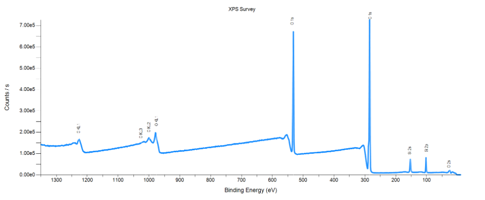
- Elemental composition (survey scan). A wide-energy survey spectrum (−10 eV to 1350 eV) identifies every element present from its peaks. Peaks are integrated to give the relative atomic percent of each element, normalized to 100%.
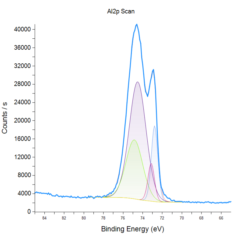
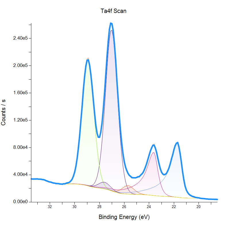
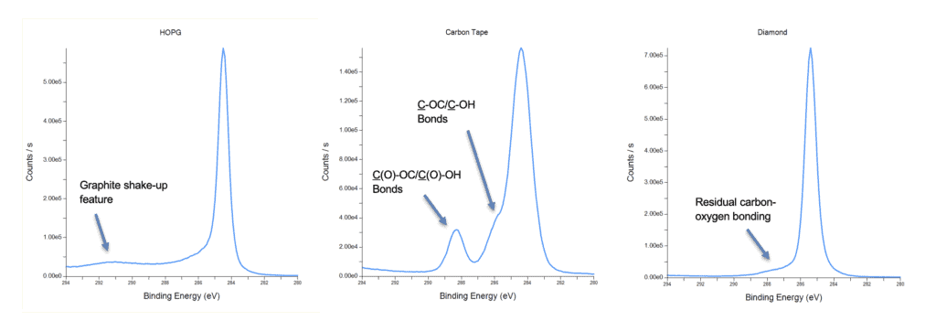
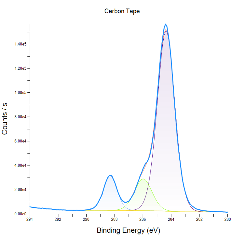
- Chemical bonding (high-resolution scans). Focused, high-resolution spectra of specific elements are fitted with peak models. The exact binding energies, compared with reference data, reveal chemical states such as metal versus oxide, or C–C versus C=O.
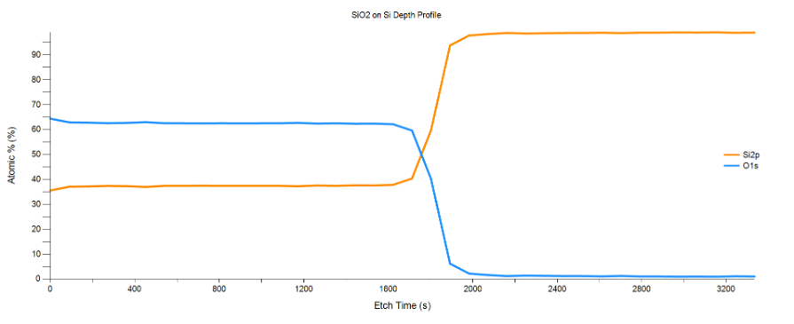
- Depth profiling. Argon ion etching removes material between measurements, showing how composition changes with depth through layers and interfaces and helping estimate layer thickness.
- Angle-resolved XPS (ARXPS). Changing the measurement angle collects information from different depths without removing material, which is ideal for very thin layers and for avoiding sputter damage.
What You Get from XPS Testing
New section, targeting "xps testing" and "xps analysis" with what buyers receive.
- Atomic percent of each element detected, with any contaminants flagged.
- High-resolution spectra with peak fits showing which chemical states are present and how much of each, such as oxide versus metal.
- Depth profiles of composition through films and interfaces, with etch rates calibrated on known standards.
- Angle-resolved thickness estimates for very thin layers, such as native oxides, without sputtering.
- Work function measurements. For valence band data, see ultraviolet photoelectron spectroscopy (UPS).
- Vacuum or inert-gas transfer for battery materials and other air-sensitive samples.
- A report from an XPS scientist that explains the results in terms of your question.
Equipment Used for XPS

ThermoFisher Nexsa
- Spot Size: 10µm to 400µm.
- Sensitivity: 0.01 atomic % to 0.5 atomic % depending on the element.
- X-ray Source: Monochromated, micro-focused, high-efficiency Al Kα X-ray Anode.
Key differentiators
Strengths
- Provides chemical bonding information from the top 7-10nm not obtainable with any other technique.
- Capable of analyzing conductors and insulators.
- Compatible with a wide variety of sample types.
- Excellent detection limits (part per thousand for some elements) and spectral resolution.
Limitations
- Does not have ppm detection limits.
- Some sample degradation can occur due to heating from x-ray or flood guns.
- Chemical bonding information is not always possible in depth profiles due to reduction of sensitive species by argon ion sputtering.
- Not suited to very rough samples.
Example Outputs
Sample Requirements
XPS can analyze any sample compatible with an Ultra-High Vacuum (10-9 mbar) including polymers, powders, cured adhesives, liquid residues, fibers, viscous oil and gels, and any other solid sample.
- Solid phase.
- Stable under ultra-high vacuum conditions.
- Max dimensions: 60 mm (L) x 60 mm (W) x 20 mm (T).
- Flatter topographies improve signal detection.
- For Powder Samples: 5-10 mg is sufficient (as long as it can cover 0.5 cm x 0.5 cm of foil or Cu tape).
XPS Applications by Industry
Semiconductor & Microelectronics
XPS detects surface contamination, and checks oxidation states that could affect device yield. XPS can measure material work functions, critical for semiconductor performance. Depth profiling verifies thin-film chemistry and reveals interlayer diffusion in multilayer stacks.
Aerospace & Defense
XPS identifies oxidation, corrosion, and contaminants on metals and coatings. It validates surface treatments and supports failure analysis of mission-critical parts, such as delaminations.
Energy & Battery Technology
XPS analyzes electrode surfaces, SEI layers, and catalyst coatings for surface contamination and oxidation states, especially effective when paired with inert gas/vacuum transfer directly into instrument.
Polymers / Coatings / Adhesives
XPS detects contamination, chemical variations, and surface treatments on polymer and coating surfaces. It supports adhesion studies and failure analysis, such as delaminations and discolorations.
Medical Devices & Biotech
XPS verifies surface cleanliness, functionalization, and bioactive coatings and surface treatments. It helps detect residues and ensure material compatibility for regulated applications.
Automotive & Industrial Manufacturing
XPS identifies corrosion products, contaminants, and wear-related chemistry. It verifies pre-coat surface quality and supports root-cause investigations.
Environmental & Catalysis Research
XPS determines oxidation states and surface species on catalysts and environmental samples. It aids in evaluating reaction mechanisms and material degradation.
Techniques That Complement XPS
Similar to XPS but making use of the Auger electron transition, initiated by electrons and not x-rays, capable of smaller (~1µm) spot sizes; best applied to depth profiling experiments. Provides limited chemical information. Similar detection limits. Not able to analyze non-conductive samples.
XPS Testing Services at Covalent
Covalent runs XPS on a Thermo Fisher Nexsa G2 in our Sunnyvale Core Lab. It has micro-focused spots down to 10 µm, vacuum transfer for air-sensitive samples, and accessories for angle-resolved and work function measurements. Our XPS scientists have more than 20 years of combined experience in XPS and materials science, so they can design the experiment around your question and tell a real peak from an overlap. Your report explains what the chemistry means for your process or failure.
Frequently Asked Questions
How do the accessories help me do different XPS experiments?
Why is having experienced XPS scientists important for understanding my results?
What types of information can XPS provide about my sample?
How should I prepare my sample for XPS to ensure reliable results?
- Avoid contact of any kind with the region of interest.
- Loosely wrap the sample in aluminum foil and secure using double sided tape to the bottom of a rigid container.
- Secure the sample to the bottom of a rigid container with the surface of interest facing up.
What is the analysis depth and spatial resolution of XPS?
- XPS analyzes the top 7-10nm of a surface.
- Spot sizes range from 10 to 400µm (elliptical) and can be adjusted in increments of 5µm.