
What Is Spectroscopic Ellipsometry?
SE measures how the polarization of light changes as it reflects from or transmits through a sample, providing information about film thickness, refractive index (n), extinction coefficient (k), and other optical constants.
SE is most often used when other methods, such as profilometry (which requires step edges) or reflectometry (often limited to only thickness measurement), cannot simultaneously determine both thickness and optical properties with the same level of accuracy. This makes SE especially valuable for complex multilayer stacks, semiconductor coatings, and thin dielectric or polymer films where material properties and layer uniformity are critical.
Other Details:
- Covers a broad spectral range (193 nm–35 µm) and film thickness range (1 Å–25 µm+).
- Advanced modeling resolves complex multilayer stacks with high precision.
- Compatible with dielectrics, metals, semiconductors, polymers, and more.
- Automated mapping stage enables high-resolution uniformity measurements across large wafers.
Non-Destructive Testing
Speed and Efficiency
Exceptional Precision and Accuracy
Why Use Spectroscopic Ellipsometry?
- Greater sensitivity to film thickness and refractive index (n) than other common optical methods.
- Can deconvolve individual layers in multilayer stacks more effectively.
- Covalent’s state-of-the-art J.A. Woollam RC2 and IRVASE ellipsometers are precise, flexible, and cover a wide range from the UV to the Far-Infrared.
Analytical Depth
Material Compatibility and Sample Size
Depth Profiling
How SE Works
A polarized light beam reflects from the sample, and changes in polarization amplitude and phase are recorded across multiple wavelengths. These changes are modeled to extract film thickness and optical constants (n, k) with high precision.
Equipment Used for SE

J.A. Woollam RC2-DI
- Spectral Range: 193 to 1690 nm (0.73 to 6.42 eV; 1075 total wavelength bands).
- Dual-rotating compensator configuration (PCRSCRA configuration).
- Automated mapping up to 300 mm substrates w/ fully customizable X-Y resolution and scan pattern.
- Measurement Beam Diameter: 5 mm (standard); or 300 µm (focused).
- Full Muller matrix measurement capability.
- Variable-angle transmission stage (45° – 90° angle-of-incidence range).

J.A. Woollam IR-VASE Mark II
- Spectral Range: 1.7 to 30 microns (333 to 5900 cm-1).
- Single-rotating compensator configuration (PCRSA configuration).
- Resolution: 1 cm-1 – 64cm-1 (user defined).
- Variable angle of incidence range: 31º – 90º
- Measurement Beam Diameter: 5mm typical, but user-reducible to ~1mm.
- Single measurement location stage with 200mm maximum sample size.
- Source / Detector: SiC Globar / DTGS
- Supports both reflection and transmission configuration measurements of standard ellipsometry, Mueller matrix ellipsometry, and transmittance/reflectance intensity.
Key Differentiators
Delivers precise, non-contact measurement of film thickness and optical properties-beyond the limits of reflectometry or profilometry.
Strengths
- Wide spectral (193 nm–35 µm) and thickness (1 Å–25+ µm) range.
- Quick, non-contact measurements, often under 10s (for RC2 measurements).
- High precision: <0.1% repeatability, ~1% of true value.
- Advanced modeling resolves complex multilayer stacks.
Limitations
- Requires smooth, flat samples for accurate results.
- Cannot measure opaque or deeply buried layers.
- Development of optical models can be time-consuming for complex projects.
Example Outputs
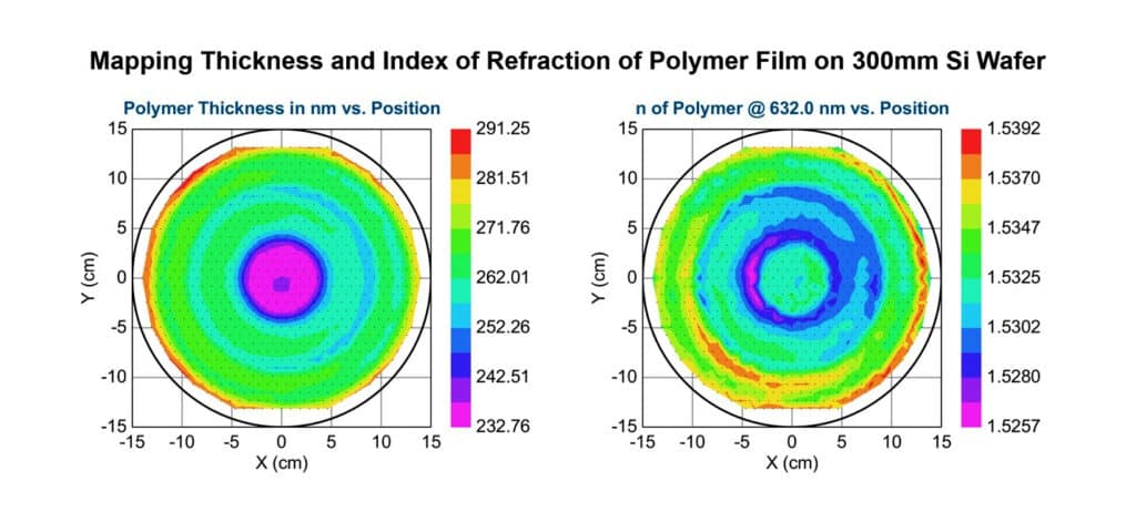
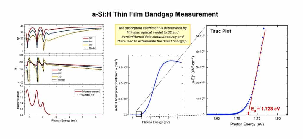
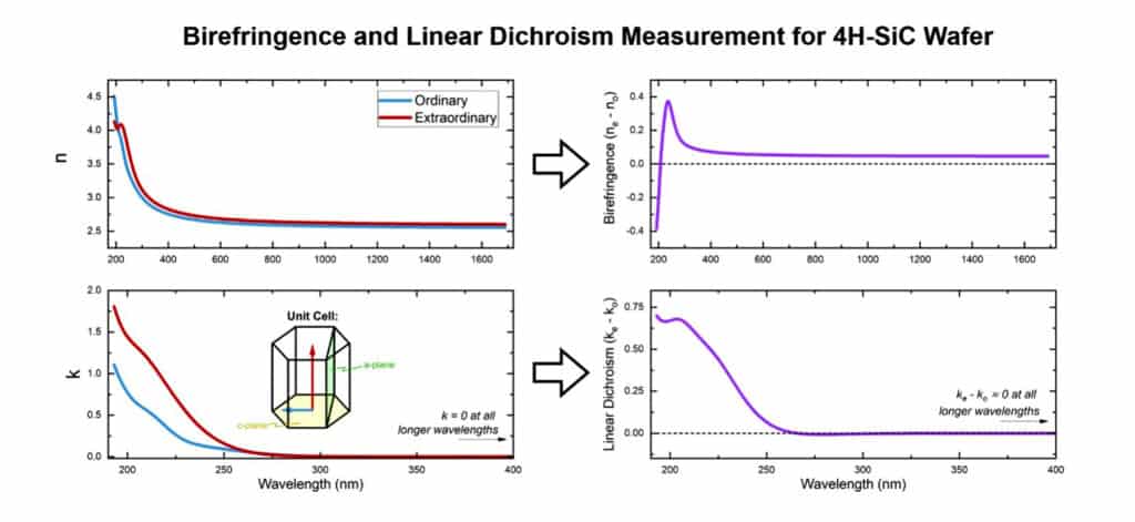
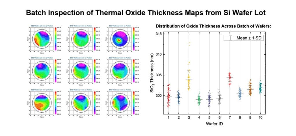
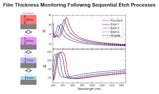
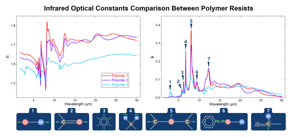
Raw spectroscopic ellipsometry measurement data are changes to the polarization state of light when reflected off a sample. The final experiment outputs are obtained by fitting optical models to the raw data to extract meaningful material properties, such as thin film thickness, optical constants, and more. The figures below provide illustrative examples of results from ellipsometry measurements.
Sample Information
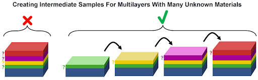
SE works best on flat, smooth samples. Sizes range from 1 mm to 300 mm, and film thicknesses range from 1 Å to 25+ µm. Films must be at least partly transparent to measure thickness. For multilayer stacks, a single SE measurement can typically only measure 2 unknown materials at once. Film stacks with many unknown layers typically require intermediate samples with partial stacks.
SE Applications by Industry
Semiconductor & Microelectronics
SE is essential in microelectronics, characterizing dielectrics, metals, and semiconductors. It precisely measures complex film stacks and helps monitor and optimize deposition and etch processes.
Energy
SE is ideal for photovoltaic (PV) applications, measuring bandgap, layer and interface thickness, and optical absorption in semiconductor absorbers and transparent conducting oxides. It also maps large-area uniformity critical to PV fabrication.
Display & Optoelectronics
SE enables precise analysis of thin film stacks that form the base of displays and sensors. It accurately measures optical coatings, color filters, and absorber layers used in optoelectronic devices.
Biomedical
SE is one of the few techniques capable of measuring ultra-thin self-assembled monolayers (SAMs) and silanized surfaces. It’s also well-suited for characterizing hydrogels, parylenes, PEG, fluoropolymers, and polymer brushes.
Polymers
SE characterizes optical properties, thickness, and surface gradients in polymer films, helping assess curing behavior, optical uniformity, and coating coverage.
Techniques That Complement SE
Why Choose Covalent for Your SE Needs?
At Covalent, our spectroscopic ellipsometry experts bring decades of hands-on experience with diverse materials and complex sample configurations. We’ve supported hundreds of customers with customized SE solutions, delivering precise, project-specific insights across various industries. Covalent also has a strong partnership with our instrument manufacturer, the J.A. Woollam Company, which is widely recognized as the premier ellipsometer manufacturer in the world.