
What Is SNOM-Raman?
SNOM‑Raman (Scanning Near‑field Optical Microscopy combined with Raman Spectroscopy) focuses a laser into a 100 nm nanoscale aperture on a specially designed probe to generate near‑field light.
This light irradiates the nearby sample, enabling acquisition of Raman spectra with spatial resolution down to 100 nm—far beyond traditional Raman—making it ideal for mapping stress and chemical structure in semiconductors and ceramics at the nanoscale.
Other Details:
- Enables nanoscale chemical imaging of complex surfaces.
- High-resolution mapping for microeletronics reliability.
- Supports cross-sectional stress analysis in devices.
- Compatible with multi-layered semiconductor structures.
Non‑Destructive and Correlative
Interface-Sensitive Insights
100 nm True Near-Field
Why Use SNOM-Raman?
- Much higher spatial resolution than conventional Raman spectroscopy.
- SNOM-Raman is a powerful technique when the spatial resolution of conventional micro-Raman spectroscopy, typically on the micrometer scale, is insufficient.
- Common Applications: Evaluation of stress and chemical structure for semiconductors and ceramics sample.
Nanoscale Stress Quantification
Cross‑Section Depth Mapping
Semiconductor and Ceramic Optimized
How SNOW-Raman Works
Spatially resolve stress by measuring Raman peak shifts with 100 nm resolution. Scan semiconductor or ceramic solids, including cross‑sections, to build depth profiles. Hold the specimen flat and smooth; this ensures compatibility with the AFM probe and delivers results far more precise than conventional Raman methods.
Equipment Used for SNOW-Raman

Horiba AFM-Raman
- Measurements are conducted using an original probe developed by Toray Research Center.
- A 355 nm laser is available as an excitation source.
- High spectral resolution (multi-grating, auto-switching) across wide Raman/PL ranges.
- High spatial resolution: Nanoscale spectroscopic resolution (down to 10 nm) through Tip Enhanced Optical Spectroscopies (Raman and PhotoLuminescence).
- Multi-mode SPM (AFM/cAFM/KPFM/STM), liquid cell and electrochemical environment, together with chemical mapping through TERS/TEPL. Full control of the 2 instruments through one workstation and a powerful software control, SPM and spectrometer can be operated simultaneously or independently.
Key Differentiators
SNOM-Raman offers 100 nm spatial resolution for precise stress mapping, enabling non-destructive analysis of semiconductors and ceramics. It captures nanoscale strain and chemical structure details beyond conventional Raman limits.
Strengths
- Stress measurement with a spatial resolution of 100 nm enabled by Toray Research Center (TRC)’s originally developed probe.
- Stress evaluation of semiconductors and ceramic samples.
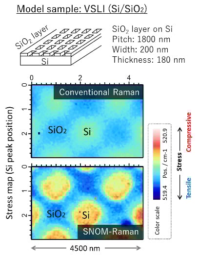
- SNOM-Raman has 100 nm spatial resolution, being much higher than that of conventional Raman spectroscopy with a micrometer scale. This high spatial resolution enables stress evaluation in patterned some real semiconductor devices.
Limitations
- Materials with vibrational modes of low Raman activity are not well suited to this technique.
- This technique can be applied to materials exhibiting vibrational modes with high Raman activity, such as semiconductors and ceramics.
Example Outputs
Sample Requirements
We accept only solid samples that are ≤ 10 mm × 10 mm in planar size and no thicker than 10 mm. The sample surface must be flat and smooth to support stable AFM probe scanning without topographical artifacts or tip damage.
SNOM-raman Applications by Industry
Semiconductor
SNOM-Raman enables precise mapping of local stress in semiconductor devices with 100 nm resolution, revealing strain patterns in Si and SiO₂ layers that conventional Raman cannot detect, supporting reliability and failure analysis in microelectronics manufacturing.
Ceramic
This technique evaluates stress and chemical structure in advanced ceramics, providing nanoscale insights into microstructural features, defects, and strain distribution, critical for industries such as aerospace, electronics, and high-performance materials research.
Microstructure
SNOM-Raman maps stress in patterned or microfabricated surfaces, such as grids or complex device layouts, enabling engineers and researchers to identify local strain concentrations and optimize design, performance, and material integrity.
Multilayer Devices
By measuring cross-sectional samples, SNOM-Raman reveals depth-resolved stress and structural variations in multilayer semiconductor or ceramic devices, aiding in the development of next-generation electronics and layered material systems.
Chemical Mapping
SNOM-Raman pairs with conventional micro-Raman spectroscopy to provide both high spatial resolution and sensitive chemical detection, supporting research fields that require nanoscale chemical imaging alongside bulk material characterization.
Techniques That Complement SNOW-Raman
Why Choose Covalent for Your SNOM-Raman Needs?
Covalent provides non-destructive SNOM-Raman analysis with 100 nm resolution for nanoscale stress and chemical mapping. Built on AFM-Raman with 355 nm excitation, our approach delivers co-registered topography and Raman data for patterned semiconductors, ceramics, multilayer stacks, and device cross-sections.