
What Is Photo-induced Force Microscopy (PiFM)?
Photo-induced Force Microscopy (PiFM) is a cutting-edge technique that combines Atomic Force Microscopy (AFM) with tunable infrared (IR) lasers to achieve nanoscale surface analysis. This hybrid approach enables researchers to capture a sample’s topography and chemistry with unmatched spatial resolution, down to a few nanometers.
While PiFM refers to the microscopy technique, mapping nanoscale structures and chemical composition, its companion, PiF-IR (Photo-induced Force IR), is used for spectroscopy. PiF-IR provides nanoscale IR absorption spectra (like FTIR does at the macroscale). The critical difference is in scale:
- FTIR spectra reflect the average macroscopic chemical environment, smoothing over nanoscale variations.
- PiF-IR spectra capture the local chemical condition at ~5 nm, revealing chemical heterogeneity that FTIR misses.
Non-Destructive and Non-Contact
Sub-5nm Resolution
Simultaneous AFM and IR Data
Why Use PiFM?
Photo-induced Force Microscopy (PiFM) provides unmatched nanoscale chemical and topographical analysis with sub-5nm resolution, enabling the detection of ultrathin layers, nanoscale defects, and chemical heterogeneity that conventional methods miss. Its non-destructive, non-contact approach works on sensitive materials like polymers, semiconductors, and biomolecules, delivering high-resolution, actionable data for research, quality control, and advanced material development.
Key Technical Parameters:
- Simultaneous IR data and AFM data.
- AFM for the usual topographic information of the sample surface.
- IR produced spectral data of the surface.
- PiF-IR spectra.
- PiFM image at a fixed wavenumber.
Material Compatibility:
- Organic, Inorganic, and biological materials.
- IR absorption cannot identify pure metals. However, other metal-based inorganic materials can be identified (e.g., metal oxides).
Spatial Resolution:
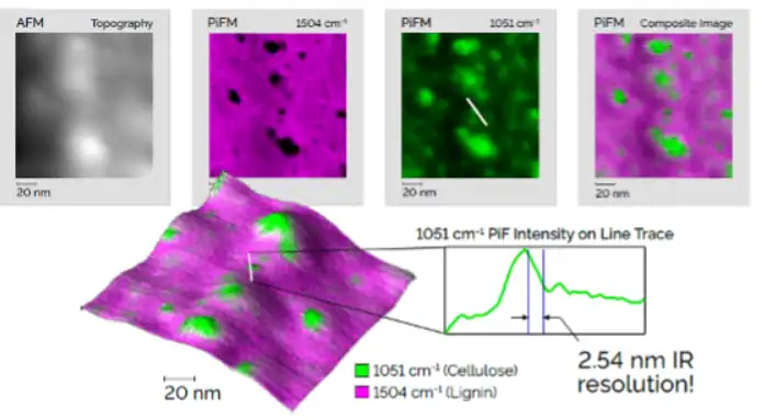
- Sub-5nm spatial resolution for chemical analysis.
- Use PiFM if conventional or well-established techniques do not provide enough nano-chemical spatial (or depth) resolution. Use PiFM if other techniques were tried first, then move to SEM or ToF-SIMS, etc.
- The techniques mentioned are applicable only if the sample is known to have nano-chemical structures beyond those techniques.
Detect Nanoscale Defects
Broad Material Compatibility
Actionable Insights
How Photo-induced Force Microscopy Works
A pointed, metal-coated probe in PiFM – whose tip radius can be as small as 20 – 30 nm after the metal coating is applied – is set very close to the surface of the sample. The area immediately underneath the tip is illuminated by an exactly focused laser beam, which creates a localized electromagnetic near field. The near field then acts on the sample’s molecule, creating localized polarization based on the optical and chemical characteristics of the material.
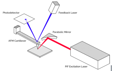
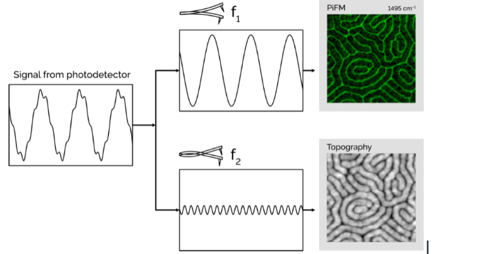
This interaction between the tip and the polarization sample generates an extremely minute attractive dipolar force, which we refer to as the photo-induced force. The laser is modulated at a specific frequency so that the AFM probe can act as a mechanical amplifier of the photo-induced force. In scanning the tip across the surface and measuring these forces continuously, PiFM generates high-resolution maps that register surface topography and spatially resolved chemical contrast in parallel. We can keep the tip stationary and sweep the laser to collect a PiF-IR point spectrum.
Equipment Used for PiFM

Vista 150 by Molecular Vista
- PiF Laser: QCL (770 to 1840, 1995 to 2395 cm−1).
- Stage and scanner:
- Sample stage travel: 150 mm × 150 mm square.
- Scan size: 90 µm × 90 µm.
- Dual Z Feedback: 12 µm z-scanner (sample) with 600 nm fast-z scanner (tip) provides both high bandwidth and a large z-range.
- Functionality:
- Imaging modes: Non-contact AFM, PiFM, KPFM, cAFM, nano DMA, FvD (force vs distance) mapping.
- Spectroscopy modes: PiF-IR, FvD.
- There are two basic modes:
- Surface Mode: measures up to 20 nm of depth of material.
- Bulk Mode: measures up to 1000 nm of depth of material.
Key Differentiators
Strengths
No other technique can provide such nanoscale (and some sub-nano) resolution in a non-destructive and non-contact manner for surface analysis, for samples in ambient air conditions with relatively ease of use compared to conventional techniques.
- Surface chemistry and topography at nanoscale resolution.
- Surface chemistry and topography at single-digit nanoscale resolution.
- Ability to measure chemical information (not elemental).
- Non-contact and non-destructive, even more than SEM/EDS.
- Ability to measure in ambient air environments.
- Full-size wafer compatibility.
- Minimal or no sample preparations.
- Ease of use (vs. similar techniques) for nanoscale chemical measurements.
Limitations
- Not well suited to pure metals and some 2D materials without IR-active peaks.
- Accessibility of the sample surface is limited by the probe’s dimensions.
- Due to the mechanical scanning, the imaging mode can be considered slow compared to optical and even electron microscopes.
With Covalent’s diverse instrumentation and its technical team’s extensive technical experience and know-how, PiFM is a strong complementary capability that enhances Covalent’s value proposition to customers.
Example Outputs
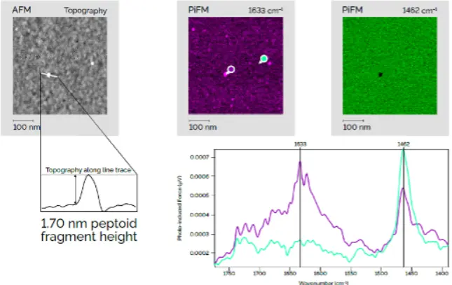
- IR spectral data – chemical information similar to FTIR output.
- AFM images & topography.
- PiF-IR images & chemical mapping.
- Single wavenumber (WN) image.
- Multiple WN images overlaid.
Sample Requirements
- Physical form: Solids only; liquids generally not measured; gases not measured.
- Sample properties: Solids and gel-like liquids must be stable in a controlled environment.
- Sample size: From small pieces mounted on a coupon (1″ x 1″) up to 300 mm wafers.
Others:
- Sample Storage/Transport: PiFM is surface sensitive enough to detect a monolayer of molecules. Do not use Gel-Pak sample containers when shipping, as they will outgas and contaminate the sample surface. Use Fluoroware or Natural Polypropylene. Please use metal tapes with acrylic adhesive if the sample needs to be secured for transport.
Photo-induced Force Microscopy Applications by Industry
Semiconductor Defect Analysis
PiFM detects sub-5nm defects and ultrathin residues without damaging sensitive wafers, making it indispensable for chipmakers and equipment suppliers seeking reliable nanoscale process validation and failure analysis.
Polymer & Materials Science
Life Sciences & Biology
Pharmaceutical Development
Energy & Nanotechnology
Techniques That Complement PiFM
Why Choose Covalent for Your PiFM Needs?
Photo-induced Force Microscopy (PiFM) testing services at Covalent deliver non-destructive, high-resolution nanoscale chemical and topographical analysis with sub-5nm precision. Ideal for semiconductors, polymers, biomaterials, and thin films, our service uncovers defects, maps chemical composition, and provides actionable insights that conventional techniques often miss.