
What Is Transmission Electron Microscopy (TEM)?
Transmission Electron Microscopy (TEM) is an imaging technique where a high-energy electron beam (typically ~200kV) is transmitted through a sample thinner than 100 nm. An image is formed by the interaction of electrons with the atoms in the sample.
Abbreviations:
- BFTEM: Bright-Field TEM.
- HRTEM: High-Resolution TEM.
- DF-TEM: Dark Field TEM.
- STEM: Scanning TEM.
- EDS: Energy Dispersive Spectroscopy.
- EELS: Electron Energy Loss Spectroscopy.
- SAD: Selected Area Diffraction.
- PED: Precision Electron diffraction.
Comprehensive Material Analysis
Multi-Mode Imaging
Atomic-Scale Resolution
Why Use TEM Analysis?
TEM is the best technique to study crystal defects, grain boundary interactions, and dislocation analysis, as we can visualize the atomic arrangement directly.
TEM provides information at the atomic scale, providing very high accuracy of measurements. It is often used instead of SEM when a better resolution is needed, and instead of X-ray diffraction, when we want to study local structural information of the crystal/defects.
Unmatched Precision
Failure Analysis and QC
Cross-Industry Applications
How TEM Works
In a TEM, a high-energy electron beam is applied to a very thin sample (a lamella), which is prepared to be electron-transmissive i.e. typically 20 to 50 nm thick.
As the beam passes through the sample, scattering interactions occur between its electrons and the atoms present, which alter the intensity of the transmitted beam. These scattering events can produce several types of contrast in the final image, including: amplitude contrast (arising from atomic number and mass/thickness), phase contrast (from quantum phase shifting due to multiple scattered beams’ interference), diffraction contrast (from crystal structure and orientation), and more.
Different imaging modes on the TEM can target specific types of contrast over others, facilitating specialized analysis of relevant information.
From the images, we can obtain layer thickness measurements, morphology, shape, and size of the nanoparticles, as well as any inclusions (defects) or delamination of the layers.
Equipment Used for TEM Analysis
We use the Talos™ F200X G2 TEM with Super-X EDS system and JEOL JEM-F200 Multi-purpose Electron Microscope for all our Transmission Electron Microscopy needs.

ThermoFisher Scientific Talos F200X G2 TEM/STEM
- Electron Source: X-CFEG (High-Brightness Field Emission Gun)
- Accelerating Voltage: 200 kV
- TEM Point Resolution: ≤0.10 nm
- STEM Resolution: ≤0.16 nm
- EDS System: Super-X with 4 SDD detectors for fast 2D/3D elemental mapping
- EELS Energy Resolution: ≤0.3 eV (X-CFEG)
- Camera: Gatan OneView CCD, 16MP / 4K
- Maximum Tilt Angle: ±35° alpha / ±30° beta (double tilt holder)
- Maximum Diffraction Angle: 24°
- Software: Velox (automated workflows and large-area analysis)

JEOL JEM-F200 Multi-purpose Electron Microscope
- Electron Source: Cold-Field-Emission Gun (CFEG)
- Accelerating Voltage: 80 kV or 200 kV
- TEM Point Resolution: 0.19 nm
- STEM-HAADF Resolution: 0.14 nm
- EDS System: Dual large-area SDD detectors for high-sensitivity mapping
- EELS Energy Resolution: <0.33 eV (cold-FEG)
- EELS Capabilities: Fine structure/oxidation state analysis, plasmon resonance, zero-loss peak
- Energy Filter: Gatan GIF Continuum ER (EFTEM)
- Modes: TEM, STEM, EDS, EELS (rapid switching)
Key Differentiators
| Property | TEM |
|---|---|
| Common Applications | Layer thickness measurements, critical dimension (CD) and gate oxide analysis, interface quality assessment, dislocation density/type studies, crystal structure and orientation analysis, nanoparticle/nanowire/nanotube/quantum dot imaging, defect origin and location identification. |
| TEM vs STEM | TEM uses a nearly parallel electron beam for full-field imaging; ideal for crystal structure and diffraction analysis. STEM uses a focused convergent beam scanned point by point; better for localized EDS/EELS analysis. |
| Analytical Depth | Measures particle morphology (size, shape, distribution), grain and pore sizes, layer thickness at sub-nanometer resolution, defects (point defects, dislocations, stacking faults, interfaces, grain boundaries), lattice structure, crystal orientation, and 3-D tomography of particles or defects. |
| Material Compatibility | Metals, semiconductors, polymers, glass, and other materials that withstand high-energy electron beams. |
| Spatial Resolution | Sub-nanometer resolution. |
Strengths
- TEM is a very high-resolution technique, which has 10-20 times better resolution than SEM. TEM is for atomic scale imaging, SEM is for nano-scale imaging.
- TEM can measure layer stacking with much more precision than SEM.
- Interface quality of the layers can be imaged at atomic level which is not possible by SEM.
- TEM is good for studying dislocations, grain boundaries, crystallographic information which is not possible by regular SEM imaging.
- TEM is used for its better resolution capabilities and reliability in measurements.
Limitations
- Destructive technique.
- Elaborate sample preparation.
- Beam sensitive materials, biological samples not suited.
- Expensive tools.
- Information comes from a small portion of the sample. Need to do multiple samples for statistical analysis.
Example Outputs
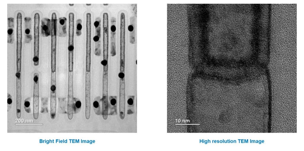
Sample Requirements
- Vacuum stable bulk samples, either conductive for FIB-based lamella preparation or samples can be coated with metal onsite at Covalent to mitigate charge artifacts during prep.
Or, if you’d like to prep the samples yourself: thin, electron-transparent lamella with a thickness of less than about 100nm.
TEM Applications by Industry
Semiconductor Equipment
TEM enables critical dimension measurements and gate oxide analysis for next-generation fabrication tools. Advanced imaging reveals equipment-induced defects and contamination sources at atomic resolution, ensuring manufacturing precision and yield optimization.
Semiconductor Manufacturing
Layer thickness validation and epitaxial interface quality assessment drive process control in semiconductor manufacturing. TEM identifies dislocation origins, stacking faults, and dopant distribution patterns critical for device performance and reliability.
Consumer Electronics
Miniaturization demands in consumer electronics require precise analysis of interconnects, solder joints, and component interfaces. TEM characterizes failure mechanisms in flexible displays, memory devices, and power management circuits.
Battery & Energy Storage
Electrode material degradation, solid electrolyte interfaces, and lithium dendrite formation analysis optimize battery performance. TEM reveals structural changes during cycling, enabling development of safer, longer-lasting energy storage systems.
Aerospace & Defense
Critical component reliability in extreme environments requires atomic-scale defect analysis. TEM characterizes superalloy microstructures, coating adhesion, and fatigue crack initiation in turbine blades and structural components.
Metallurgy
Grain boundary engineering and precipitation hardening mechanisms benefit from TEM’s crystallographic analysis capabilities. Phase transformation studies and corrosion interface examination guide alloy development for industrial applications.
Techniques That Complement TEM
TEM Testing Services at Covalent
Advanced TEM analysis combines cutting-edge JEOL JEM-F200 instrumentation with sub-nanometer resolution capabilities and ultra-high-energy-resolution EELS (<0.36 eV). Simultaneous HAADF/BF-STEM imaging delivers comprehensive structural characterization from multiple contrast modes.
Covalent's experienced cross-industry team provides exceptional data quality within 24-48 hours, accelerating your research timelines.