
What Is Scanning Transmission Electron Microscopy?
Scanning Transmission Electron Microscopy (STEM) is a hybrid electron microscopy technique that combines the advantages of SEM and TEM. Unlike conventional TEM, the electron beam is focused on a sub-nanometer-sized probe and scanned across the sample to form a STEM image.
Z-Contrast Imaging
Atomic Resolution
Chemical Precision
Why Use STEM?
STEM is useful for atomic-scale imaging, as STEM images can provide information on layer thickness, investigate defects and interfaces, provide grain boundary information, and provide Z-contrast imaging.
While TEM and STEM can be used for atomic-scale imaging, STEM has an advantage when imaging samples containing different atomic numbers. For EDS/EELS analysis, STEM mode provides precise beam control, making it a better technique for this case.
Defect and Interface Insight
Layer Thickness and Composition Control
Superior Failure Analysis
How STEM Works
- Lamella preparation: sample prep by FIB-SEM to under 100 nm thick.
- The probe: a probe focused below 1 nm that rasters across the lamella.
- The detectors: bright-field, ADF, and HAADF detectors, and why HAADF contrast scales with atomic number. Heavier elements appear brighter.
- Spectroscopy: EDS and EELS spectra collected at each point to build composition and bonding maps.
STEM vs TEM: Which Do You Need?
| TEM | STEM | |
|---|---|---|
| Beam | Parallel, full-field | Focused probe, scanned |
| Best for | Diffraction, crystal structure, dislocations | Z-contrast, EDS/EELS chemical maps |
| Layer contrast | Thickness and diffraction | Atomic number (HAADF) |
Equipment Used for STEM

ThermoFisher Scientific Talos F200X G2 TEM/STEM
- Electron Source: X-CFEG (High-Brightness Field Emission Gun)
- Accelerating Voltage: 200 kV
- TEM Point Resolution: ≤0.10 nm
- STEM Resolution: ≤0.16 nm
- EDS System: Super-X with 4 SDD detectors for fast 2D/3D elemental mapping
- EELS Energy Resolution: ≤0.3 eV (X-CFEG)
- Camera: Gatan OneView CCD, 16MP / 4K
- Maximum Tilt Angle: ±35° alpha / ±30° beta (double tilt holder)
- Maximum Diffraction Angle: 24°
- Software: Velox (automated workflows and large-area analysis)

JEOL JEM-F200 Multi-purpose Electron Microscope
- Electron Source: Cold-Field-Emission Gun (CFEG)
- Accelerating Voltage: 80 kV or 200 kV
- TEM Point Resolution: 0.19 nm
- STEM-HAADF Resolution: 0.14 nm
- EDS System: Dual large-area SDD detectors for high-sensitivity mapping
- EELS Energy Resolution: <0.33 eV (cold-FEG)
- EELS Capabilities: Fine structure/oxidation state analysis, plasmon resonance, zero-loss peak
- Energy Filter: Gatan GIF Continuum ER (EFTEM)
- Modes: TEM, STEM, EDS, EELS (rapid switching)
Key Differentiators
While both TEM and STEM deliver atomic‑scale insights, each has its own strengths and trade‑offs. Understanding their differences helps in choosing the right technique for specific materials and analytical goals.
Strengths
- Covalent has a cold FEG TEM, which has better EELS energy resolution.
- Precise control of the beam in STEM is very helpful for collecting EDS/EELS.
- STEM provides exceptionally good Z-contrast imaging, which is a much better way to visualize the layers when they have different average atomic numbers.
- STEM is the chosen technique for customers interested in dislocation analysis or chemical composition information.
Limitations
- Expensive tools.
- Destructive technique.
- Elaborate sample preparation.
- Beam-sensitive materials and biological samples are not suited.
- Information comes from a small portion of the sample; multiple samples are needed for statistical analysis.
Example Outputs
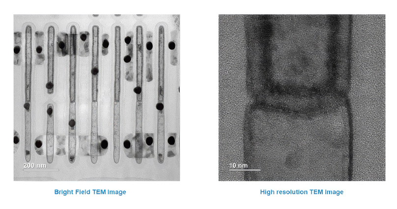
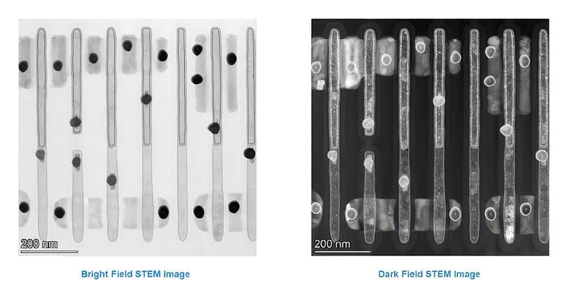
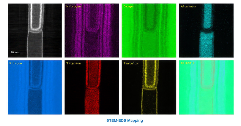
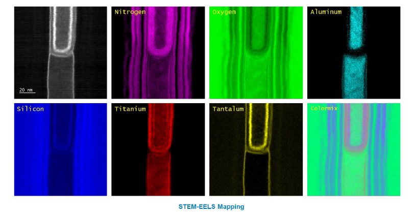
This image exemplifies a Toshiba chip, where a STEM lamella is prepared to understand the structure's layout. TEM, STEM/EDS/EELS data is provided, where STEM images clearly show the Z-contrast information that is missing in the TEM images. EDS and EELS data are provided, showing the 2-D distribution of the elemental composition. EDS and EELS are complementary techniques, and we can choose one or the other depending on the elements of interest and the resolution needed. EELS usually has better resolution than EDS.
Sample Requirements
- Thin transparent lamella with a thickness below 100 nm.
- Electron transparency.
- For a 2 mm sample size, the elemental composition has to be at least 1 at.% to be detected by EDS or EELS.
- Samples should be conductive for lamella preparation.
STEM Applications by Industry
Semiconductor
- Used for thin film analysis, defect characterization, and material interfaces.
- Used for nanometer-scale wafer defect analysis to determine which part of the layer stack the defect originates from and its composition using STEM/EDS or STEM/EELS.
Defense & Aerospace
Atomic resolution of grain boundaries and precipitates, interface reactions at the nanoscale for coatings.
Consumer Electronics
Measurement of channel, electrode length, and oxide thickness, including high-k and metal electrodes in FinFET or other latest logic devices.
Battery Research
Used for electrode morphology, degradation mechanisms, and elemental mapping.
Failure Analysis
Used for defect localization, structure and interfaces, and cross-sectional imaging.
Techniques That Complement STEM
TEM reveals crystal structure and defects across a wide area, while STEM adds Z-contrast and EDS/EELS chemical mapping. Together they deliver structure and chemistry from the same lamella.
Provides surface chemistry and oxidation states of the elements, offering complementary analysis to the elemental information from STEM/EDS or EELS.
STEM Testing Services at Covalent
Our team at Covalent has experience analyzing samples from various industries. We use high-end STEM tools with sub-nanometer resolution. Our team can provide high-quality data within 2-3 days TAT, sometimes less than 24 hours.
Frequently Asked Questions
How does Scanning Transmission Electron Microscopy (STEM) compare to Transmission Electron Microscopy (TEM)?
What is the role of EDS and EELS in STEM analysis?
EDS maps which elements are present and is fast for heavier elements. EELS adds better resolution for light elements, plus bonding and oxidation-state information.
Can STEM be used to analyze both conductive and non-conductive materials?
What types of microscopy techniques are used in STEM for elemental mapping?
Can STEM provide elemental mapping?
What is HAADF in STEM?
HAADF (high-angle annular dark-field) imaging collects electrons scattered to high angles, so brightness scales with atomic number. It shows heavy and light layers clearly, without the diffraction artifacts of conventional TEM.