Covalent

Scanning Capacitance Microscopy (SCM)

SCM is a scanning probe microscopy technique that maps charge carrier polarity and distribution in semiconductors with sub-100nm resolution. It evaluates carrier concentrations from 1e16-1e20 cm⁻³ through dC/dV signals, ideal for SiC-MOSFET and IGZO-TFT analysis.

What Is Scanning Capacitance Microscopy (SCM)?

Scanning Capacitance Microscopy (SCM) is a specialized scanning microscopy technique that provides detailed information about charge carrier in semiconductors with sub-100nm resolution.

SCM evaluates carrier concentration by measuring the local capacitance, namely dC/dV, under an applied AC voltage between the conductive AFM tip and the sample. This technique simultaneously acquires AFM images, enabling direct correlation between electrical properties and device structure for comprehensive semiconductor analysis.

Correlated Imaging

Combines AFM topography with electrical data for complete device insight.

Analytical Depth

Maps carrier polarity and concentration beneath the device surface.

Resolution

Sub-100nm spatial resolution for carrier mapping in semiconductors.
The above graph shows the measurement of the local capacitance under an AC bias voltage to the sample using an AFM probe; the carrier polarity and carrier concentration can be evaluated through the dC/dV signal.

Why Use SCM?

  • Advanced sample preparation techniques support high data reliability.
  • Although STEM-EDX helps detect impurities with a 1e21 cm⁻³ concentration or more, SCM is necessary for concentrations below 1e20 cm⁻³.
  • Evaluates charge carrier polarity and concentration with a sub-100nm resolution.

Analytical Depth

Carrier distribution maps and semi-quantified carrier concentration line profiles.

Material Compatibility

Semiconductors with carrier concentrations of 1e16 cm⁻³ to 1e20 cm⁻³.

Depth Profiling

Any depth region can be accessed using a cross-sectional sample.
Cross-sectional SCM image showing carrier distribution in a semiconductor device. The dC/dV signal differentiates between n-type (blue, negative dC/dV) and p-type (pink/red, positive dC/dV) regions beneath the gate metal structure. Scale bar represents 1μm, demonstrating SCM’s ability to map carrier polarity and spatial distribution with high resolution.

How Scanning Capacitance Microscopy (SCM) Works

SCM utilizes an AFM probe to measure local capacitance changes under AC bias voltage. The technique generates dC/dV signals that directly correlate with carrier polarity and concentration. Cross-sectional specimens enable depth profiling in any region of interest. Simultaneous AFM imaging provides structural correlation with electrical properties. Advanced sample preparation ensures reliable data from 1E16 to 1E20 cm⁻³ carrier concentrations.

Equipment Used for SCM

Bruker Dimension XR (SCM option), NanoScope V

  • AFM platform: Large-sample SPM with PeakForce Tapping for routine atomic-defect and sub-nanometer imaging in air and liquid.
  • Nanomechanics: AFM-nDMA for quantitative nanoscale storage/loss modulus over 0.1 Hz–20 kHz, linked to bulk DMA.
  • Nanoelectrical: DataCube modes for hyperspectral electrical mapping, giving electrical and mechanical spectra at every pixel.
  • Nanoelectrochemistry: PeakForce SECM / EC-AFM for <100 nm-resolution electrochemical imaging with simultaneous topography, electrical, and mechanical contrast.
Specifications

Key Differentiators

SCM provides direct feedback on fabrication processes for impurity injection verification. The technique offers exceptional sensitivity for low-concentration carriers below 1e20 cm⁻³ where other methods fail.

Strengths

  • Detects carrier polarity and detects small amounts of charge carriers.
  • Provides direct feedback on the fabrication process.
  • Highly reliable experimental data due to Covalent’s advanced technique.

Limitations

  • Not for metals or insulators.
  • Best resolution: 20 nm (decreases at low concentration); max area 80×80 μm².
  • Higher carrier sensitivity, but lower spatial resolution than STEM-EDX.

Example Outputs
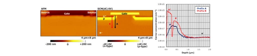
Carrier distribution in SiC-MOSFET and semi-quantified carrier concentration profile along the arrows shown in the figure.
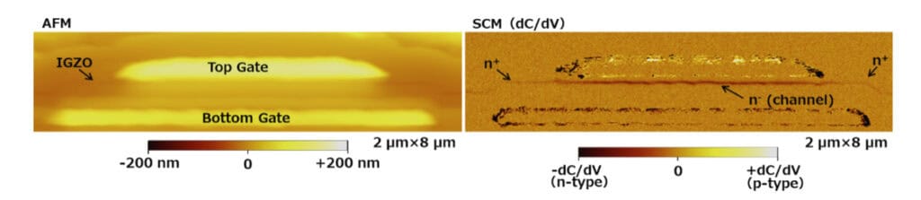
The figure above shows the carrier distribution in IGZO-TFT for evaluating the relationship between gate length and channel length.

Sample Requirements

  • Semiconductor sample (patterned device or wafer).
  • Semiconductors with carrier concentrations of 1e16 cm-3 to 1e20 cm-3.
  • The sample area of interest should be larger than 0.5×0.5 μm2.
  • Cross-sectional sample preparation is necessary for SCM measurements.

SCM Applications by Industry

Power Electronics

SCM characterizes wide-bandgap semiconductors like SiC and GaN in power devices that operate at high voltages and temperatures. The technique maps carrier concentration gradients in MOSFET channels and evaluates junction integrity in IGBT structures. SCM supports reliability testing by detecting early-stage degradation mechanisms in power semiconductor components.

Semiconductor

SCM enables precise metrology of p, p+, n, and n+ regions by measuring their width and thickness with nanoscale accuracy. The technique evaluates charge carrier distribution patterns critical for device performance optimization. SCM proves invaluable in failure analysis and reverse engineering by identifying dopant migration, junction degradation, and process variations.

Techniques That Complement SCM

SIMS
For impurity dopant concentration evaluation along with the depth direction.
Add to Quote
SIMS and SCM
SIMS is often combined with SCM to consider the activation rate of impurities.
Add to Quote
Used to evaluate impurity spatial distribution.
Add to Quote

Why Choose Covalent for Your SCM Needs?

Covalent delivers SCM testing with unmatched sensitivity and spatial resolution for precise carrier polarity and distribution evaluation. Our expertise extends beyond standard measurements, including optimized experimental conditions and advanced cross-sectional specimen preparation techniques. This comprehensive approach ensures highly reliable data acquisition and superior analytical results for your semiconductor characterization needs.

Frequently Asked Questions

Is it possible to quantify carrier concentrations in any type of semiconductor?

Semi-quantification is possible for Si and SiC semiconductors using our proprietary calculation models. Qualitative carrier distribution mapping and polarity identification remain available for other semiconductor materials.

What measurement error can be expected with SCM carrier concentration analysis?

The error ranges from half an order of magnitude to one order of magnitude of carrier concentration.

Can SCM differentiate between edge and screw dislocation types in materials?

No, SCM cannot.

What minimum feature size can SCM resolve in patterned semiconductor devices?

Roughly 50-100 nm.

How does ambient humidity affect SCM measurement accuracy and reliability?

SCM data is collected in the temperature/humidity-controlled laboratory room. We don’t think that the humidity is a critical problem.

Can SCM analyze buried interfaces in multilayer semiconductor device structures?

SCM can detect if the carrier concentration in the region of interest is higher than in other areas.

How accurately can SCM measure individual semiconductor layer thickness in heterostructures?

SCM can if the thickness of each layer is more than several tenth of nms.