
What Is 4-Point Probe (4PP) Measurement?
The Four-Point Probe technique offers an accurate and reliable method for measuring electrical resistivity or sheet resistance. It eliminates the effects of contact and lead resistance.
Using 4 points (as opposed to 2 points) separates current and voltage paths, reducing measurement errors. It is non-destructive, quick, and easy to perform.
The method applies to a wide range of materials, from thin films to bulk materials and across a wide range of conductivity.
Broad Applicability
Multi-Site Mapping
Kelvin/4-Wire Sensing
Why Use 4PP Measurement?
- Non-destructive testing, high sensitivity, high accuracy, and fast.
- Powerful for surface and near-surface resistivity measurements.
- Perfect for semiconductor and thin film materials.
- Go-to analysis for both industries and R&D.
Analytical Depth
Material Compatibility
Spatial Resolution
How 4PP Measurement Works
The 4PP technique uses a separate set of probes to flow current and measure voltage to eliminate the effect of contact resistance. Outer probes (1 and 4) pass a known current through the sample, and inner probes (2 and 3) measure the voltage drop.
Equipment Used for 4PP Measurement

Ossila 4PP
- Probe spacing: 1.27 mm.
- Rectangular Sample Size Range:
- Long-edge Minimum: 5 mm.
- Short-edge Maximum: 60 mm.
- Circular Sample Size Range (Diameter): 5.0 – 76.2 mm.
- Maximum Sample Thickness: 10 mm.
- Acccuracy as low as ±1% for sheet resistance in 10 Ω – 10 kΩ range.
- High reproducibility, with deviation below 1% for most measurements.
Key Differentiators
The Four-Point Probe delivers precise, non‑destructive sheet resistance and resistivity data with rapid throughput. It supports diverse materials, from semiconductors and transparent conductors to metals and polymers, and scales from spot tests to mapped surveys.
Consider the following capabilities and constraints when selecting it for your workflow.
Strengths
- Non-destructive, powerful, fast, and accurate technique for surface resistivity measurements.
- Broad material compatibility with:
- Silicon and compound semiconductors.
- Transparent conductive oxides (e.g., ITO).
- Metal films and foils.
- Graphene and 2D materials.
- Conductive polymers.
Limitations
- Lack of depth resolution.
- Surface roughness, probe alignment, and contact stability can limit effective resolution, especially at small scales.
- No fragile, small, or highly curved samples.
- Minor surface damage risk.
Example Outputs
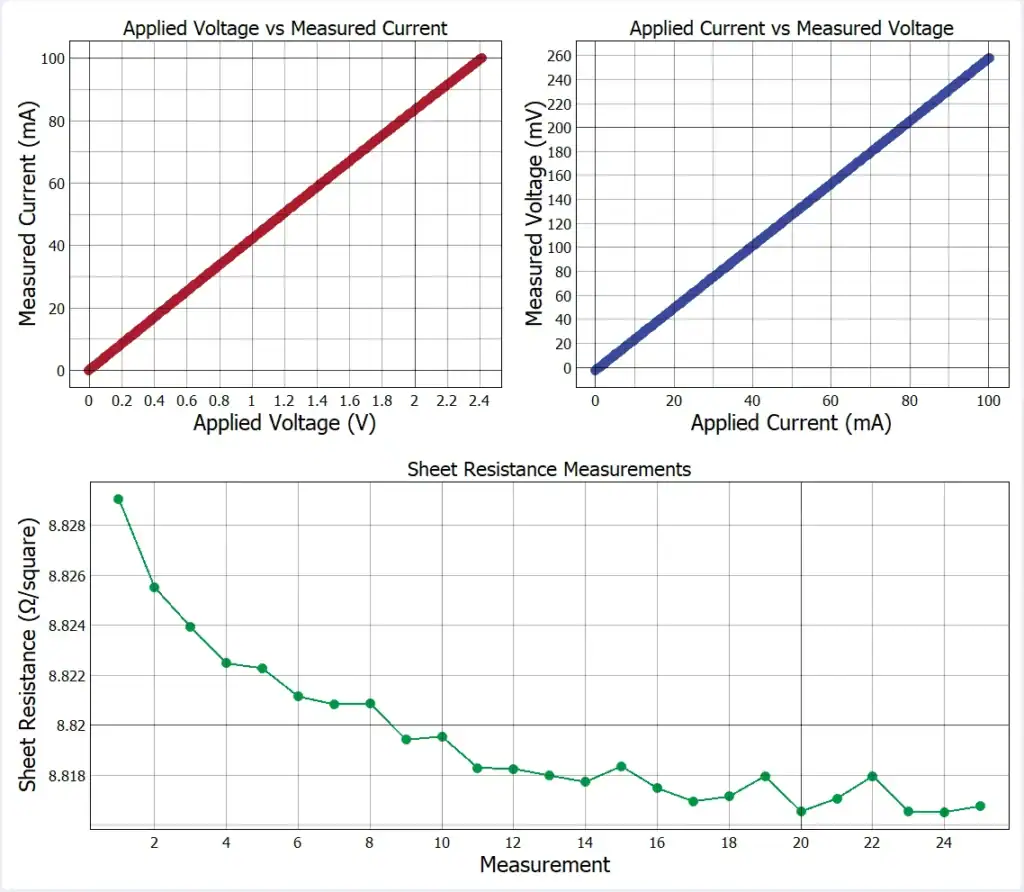
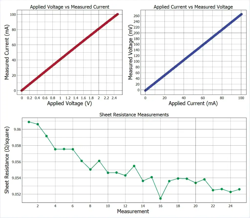
Sample Requirements
- Solid samples with a minimum of 1x1cm.
- Risk of small surface damage.
4PP Applications by Industry
Semiconductor
A semiconductor R&D team needed a fast way to measure resistivity to understand the impact of various doping recipes for silicon wafers. Covalent used 4PP to measure the sheet resistance directly on the wafers and translate it to resistivity. Our clients were able to quickly iterate the diffusion conditions, saving the client weeks using 4PP.
Display Manufacturing & Consumer Electronics
A display manufacturer needed to confirm the homogeneity of ITO coatings across glass panels used in touchscreens. Our team mapped sheet resistance at various locations. Thanks to 4PP’s quick and non-destructive QC tool, manufacturing could move forward with confidence without the need for further lithography or contact pads.
Techniques That Complement 4PP Measurement
Why Choose Covalent for Your 4PP Needs?
At Covalent, we are experts in interpreting complex data and optimizing measurements. Our advanced corrective models, specifically designed for small or abnormal geometries, ensure precise and accurate results. We also have expertise in correlating data with material, process, and application specifics, which allows us to adjust our approach to meet your unique project requirements.