
What Is Structured Light Profilometry?
Structured Light Profilometry is an optical profilometry technique in which striped patterns of light are projected down onto the sample to measure 3D surface topography. Also known as “VR” due a popular instrument, this method can reliably measure surface features 5 μm in height. Its wide measurement range extends beyond 10 mm, allowing analysis of both fine microstructures and larger dimensional variations. This balance makes it suitable for precision parts and large components alike.
High-Resolution 3D Scanning
CAD-Compatible Outputs
Wide Measurement Range
Why Use Structured Light Profilometry?
Structured Light Profilometry offers a fast, non-contact way to capture precise 3D surface data across a wide range of materials and component sizes. It delivers accurate measurements of flatness, warpage, and feature height without damaging or altering the sample. The technique’s ability to scan large areas with micrometer-level resolution makes it ideal for quality control, tooling verification, and production validation. With minimal sample preparation required, it accelerates inspection workflows while maintaining high repeatability and compatibility with CAD-based dimensional analysis.
Fast, Non-Contact Profiling
Versatile Application Range
Improved Dimensional Accuracy
How Structured Light Profilometry Works
Structured Light Profilometry is an optical profilometry technique in which striped patterns of light are projected onto the sample at a known angle of incidence. A camera overhead captures the distortion of the bands of light due to changes in the height of the sample's surface. The measured distortions are triangulated among different patterns to generate a quantitative 3D model of the surface topography. Unique to this technique, the generated 3D model is compatible for output as a CAD overlay for volumetric comparison in process and part evaluation.
Equipment Used for Structured Light Profilometry
Covalent uses the Keyence VR Wide-Area 3D Measurement System for Structured Light Profilometry. This advanced optical system captures instant 3D surface data in a single scan with high vertical accuracy and automated stitching for large fields of view. Its wide magnification range and long working distance make it ideal for profiling both fine microstructures and large, complex parts.

Keyence VR Wide-Area 3D Measurement System
- One-Shot 3D Measurements: Capture 3D CAD surface data instantly, in a single scan.
- Automated Field Stitching: Expands X-Y coverage for larger samples.
- Wide Magnification Range: 12x to 160x for varied detail requirements.
- High Accuracy: Height ±2.5 µm, width ±2 µm in High-Mag Mode.
- Flexible Height Measurement: Up to 10 mm in Wide-Field Mode, 1 mm in High-Mag Mode.
- Automated Field Stitching: Expands X-Y coverage for larger samples.
Key Differentiators
| Property | Structured Light Profilometry |
|---|---|
| 3D Surface Profiling | Captures detailed topography, flatness, warpage, and feature heights in a single scan |
| Vertical Resolution | Measures feature heights from 5 µm up to 10 mm with ±2–5 µm accuracy |
| Sample Coverage | Single field of view up to 24 × 18 × 10 mm; larger samples up to 100 × 90 × 50 mm via stitching |
| Material Compatibility | Works with most metals, polymers, composites; coatings handle reflective or transparent surfaces |
| Non-Contact Measurement | Rapid, non-destructive scanning without sample prep |
| CAD Integration | 3D models compatible with CAD overlays for part evaluation and volumetric comparison |
| Spatial Resolution | Lateral and height resolution optimized for precision parts and microstructures |
Strengths
- Compared with other optical profilometry techniques, this technique is best suited for profiling large parts with feature heights in the 5 μm – 10 mm range.
- High vertical resolution (limit < 5 μm) with balanced lateral resolution (~5 μm).
- This instrument can quickly profile surfaces in three dimensions, with a non-contact, non-destructive method that usually requires no sample prep.
- Very long working distance (75 mm) allows for profiling odd-shaped parts, which may be difficult to fit under traditional microscopy tools with shorter working distances.
Limitations
- This tool may have difficulties with very transparent or specular reflective surfaces.
- High aspect ratio dimensions block the light source.
- Better data may be achieved using an alternate optical profilometry or electron microscopy technique, depending on the sample surface and the resolution requirements.
Example Outputs
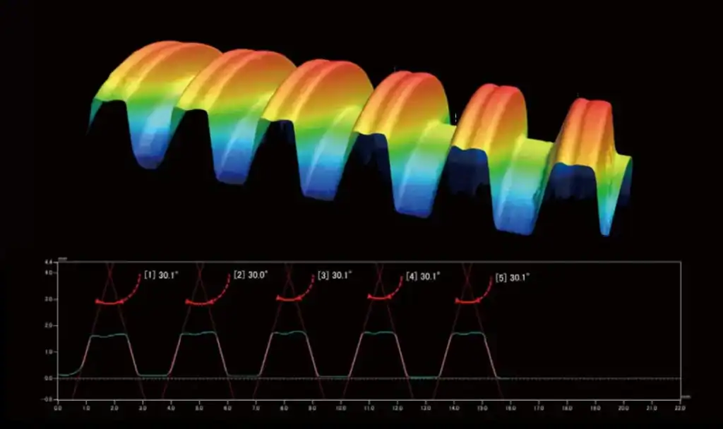
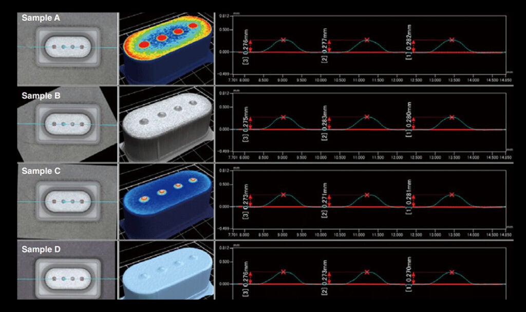
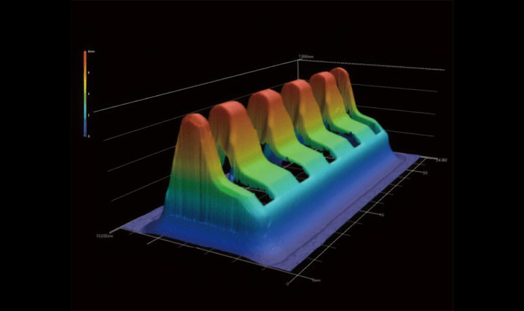
Sample Requirements
We accept samples with minimum feature sizes of 5 μm for reliable profiling. In a single field of view, surfaces up to 24 mm × 18 mm × 10 mm can be measured. Larger samples—up to approximately 100 × 90 × 50 mm—can be accommodated using image stitching.
Structured Light Profilometry Applications by Industry
Automotive / Aerospace / Electronics
Additive Manufacturing and 3D Printing
Plastics, Automotive & Consumer Electronics
Materials Science & Surface Engineering
Semiconductor & Electronics Components