
What Is Energy Dispersive X-ray Fluorescence (EDXRF)?
EDXRF is a non-destructive analysis technique used to measure elemental composition by measuring characteristic X-ray fluorescence generated when the sample is excited by X-rays.
Rapid, Non-Destructive
Wide Element Range
Hybrid Precision
Why Use EDXRF?
EDXRF provides rapid and non-destructive quantification of the composition of bulk materials and thin films, as well as measurement of film thickness and impurity levels.
EDXRF enables verification of metal film deposition, control over process drift, and identifies contamination that could affect device performance. Focused sources for XRF enable micro-spot mapping of composition variation across wafers and patterned structures. EDXRF is fast and well-suited for quick quantification of metallic and dielectric film components.
Accelerate Process Control
Support for R&D & Production
Expert-Driven Insights
How EDXRF Works
Energy Dispersive X-ray Fluorescence (EDXRF) excites atoms in the sample with X-rays and detects the energy of emitted fluorescence, providing elemental composition information. The energy of the emitted fluorescent X-rays is measured in parallel using a high-speed silicon drift detector (SDD).
Equipment Used for EDXRF
At Covalent, we offer high-precision XRF on advanced thin films and multilayer stacks using the Rigaku Xtraia MF‑3000, operated at Rigaku. This allows us to provide small-spot, whole-wafer mapping with fab-grade throughput and repeatability.

Rigaku XTRAIA MF-3000
- Covalent has a 9kW rotating anode Rigaku SmartLab that allows for higher energy X-rays than other labs.
- The Rigaku XTRAIA MF-3000 has both XRR and EDXRF capabilities allowing elemental analysis as well as thickness, density, and roughness information on the same location on a wafer as well as wafer mapping.
Key Differentiators
| Property | EDXRF |
|---|---|
| Film Thickness Range | ~1 nm to 50 µm (optical); up to ~500 nm (XRR) |
| Lateral Resolution | <1 mm |
| Wafer Size | 200 mm and 300 mm |
| Measurement Time | <2 minutes per site |
| Element Range | Al (Z=13) to U (Z=92) |
| Software | Integrated analysis and modeling tools |
| Application Range | Thickness and composition of thin films, nm to µm level |
| FEOL Applications | SiGe, CoSix, NiSix, SOI, Al, SiON, Hi-k dielectric/metal gate |
| BEOL Applications | Cu seed, Cu barrier, Cu plating, Ti/TiN, Ta/TaN, W |
| Other Applications | Ru, Pt, PZT |
| Incident Optics for XRF | Recipe-selectable COLORS™ micro spot optics, 25 W (50 kV / 0.5 mA) |
| Beam Modules | COLORS™-s (85 µm FWHM) or COLORS™-t (20 µm FWHM) |
| X-ray Sources | Cu-Kα (low-Z), Mo-Kα (high-Z), Au-Lβ (mid-Z) |
| Receiving Optics | Peltier-cooled Silicon Drift Detector (SDD) |
| Energy Resolution | 123 ± 5 eV |
| Goniometer Type | Theta-Theta goniometer (Horizontal Sample Placement) |
| Sample Stage | Vacuum chuck for ϕ300 mm or 200 mm wafers; supports coupons or smaller samples via carrier wafer |
| Sample Height Adjustment | Optical microscope with 5x lens and CCD camera for Autofocus |
| Pattern Recognition | Bright Field and Dark Field capability |
Strengths
- Combines XRR and EDXRF in a single tool.
- Non-destructive, high-throughput analysis.
- Wide range of measurable film types (metallic, dielectric, transparent).
- Sub-nanometer thickness precision.
- Automated wafer handling and mapping.
- Ideal for inline process control and R&D environments.
- Supports 200 mm and 300 mm wafers.
Limitations
- Requires flat, uniform sample surfaces for accurate results.
- Complex multilayers may require modeling for accurate interpretation.
- XRR limited to thicknesses below ~500 nm for optimal precision.
- EDXRF has limited sensitivity to Al, Mg.
Example Outputs
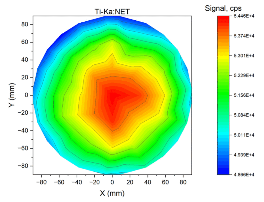
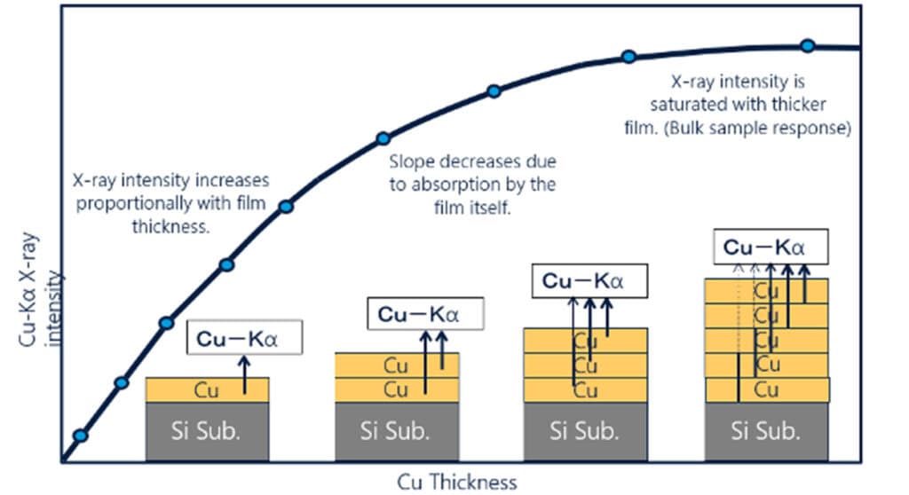
Sample Requirements
Samples must be solid materials and ideally flat. If they are not, some mechanical preparation may be required for more reliable testing. Surface roughness may need to be analyzed to determine the correct load and contact depth. As a general rule of thumb, the contact depth.
EDXRF Applications by Industry
Semiconductor
Analyze thin films, coatings, and interconnects on 200–300 mm wafers for elemental composition and thickness uniformity.
Data Storage & Electronics
Verify layer composition and detect trace contaminants in magnetic films, PCBs, and advanced storage devices.
Solar & Photovoltaics
Assess thin-film solar panels, OLED, and LCD displays for uniformity, contamination, and material quality.
R&D & Advanced Packaging
Support research labs with rapid elemental quantification, thickness mapping, and contamination analysis.
Metallurgy & Coatings
Measure alloy composition, coating thickness, and surface uniformity for quality control and process optimization.
Techniques That Complement EDXRF
Why Choose Covalent for Your EDXRF Needs?
Covalent delivers fast, non-destructive thin film and elemental analysis using high-sensitivity EDXRF instrumentation. Our capabilities include full-wafer and larger-sample handling, micro-spot mapping, and complementary material characterization techniques for demanding research and industrial applications.