
What is Total Reflection X-ray Fluorescence?
Total Reflection X-ray Fluorescence (TXRF) works by directing a collimated X-ray beam at a shallow, grazing angle onto a sample surface, typically a silicon wafer. At this low incident angle, total external reflection occurs, which restricts interaction to the near surface of the wafer. This minimizes background noise and enhances sensitivity to trace elements present on the surface. When atoms on the wafer surface are excited by the X-ray beam, they emit characteristic fluorescent X-rays, which are then detected and analyzed. The concentration of elements is quantified using reference standards.
Wafer Compatibility
Analysis Type
Detection Limit
Why Use TRXF?
TXRF is highly surface-sensitive and ideal for detecting trace metal contamination near the sample surface, because grazing incidence X-rays interact only with the top few nanometers of the sample.
The TXRF-V310 features automatic wafer handling, contamination mapping, and advanced software capable of quantifying elements at or below 1E10 atoms/cm². Its high sensitivity and repeatability enable analysis of cleaning processes, tools, and process contamination with greater accuracy and efficiency.
Surface Sensitivity
Automation & Mapping
Quantitative Accuracy
How TXRF Works
Total Reflection X-ray Fluorescence (TXRF) works by directing a collimated X-ray beam at a shallow, grazing angle onto a sample surface, typically a silicon wafer. At this incident angle, total external reflection occurs, restricting interaction to the near surface of the wafer. This minimizes background noise and enhances sensitivity to trace elements on the surface. When atoms on the wafer surface are excited by the X-ray beam, they emit characteristic fluorescent X-rays. These are then detected and used to quantify element concentrations using reference standards.
- Analytical Depth: TXRF provides quantitative information on elemental composition at the near-surface region of a sample, typically within the top few nanometers.
- Material Compatibility: This technique is compatible primarily with 200 mm and 300 mm semiconductor wafers. While silicon wafers are primarily analyzed other compound semiconductors can also be analyzed.
- Spatial Resolution: While TXRF does not offer high spatial resolution like imaging techniques, it can map contamination patterns across sample surfaces using automated stage movement with a resolution on the order of 5 -10 mm.
- Depth Profiling: TXRF is primarily a surface-sensitive technique and does not perform depth profiling for layered material analysis; it focuses on detecting elements at or near the surface.
Equipment Used for TXRF

Rigaku TXRF V310
- Elemental detection range: Na (Z=11) to U (Z=92)
- Detection limit: Approximately 1E10 atoms/cm² (element-dependent)
- Compatible wafer sizes: 200 mm and 300 mm
- Atmosphere: Vacuum or helium purge
- Measurement modes: Single-point, multi-point, and mapping analysis
- Software: Automated element quantification and contamination trend analysis
- High-power W-anode X-ray source (9 kW rotating anode)
- Three excitation energies optimized for light, transition, and heavy elements
- XYθ sample stage for precise positioning
- Dual FOUP (Front Opening Unified Pod) load ports
Key Differentiators
TXRF is a technique distinguished by its exceptional surface sensitivity, ultra-trace detection limits, and non-destructive measurement, but it also has key technical constraints.
Strengths
- Ultra-trace sensitivity (detects as low as 1E10 atoms/cm²)
- Non-destructive analysis of wafer surfaces
- Requires minimal sample preparation
- High throughput enabled by automated wafer handling
- Offers excellent repeatability and reproducibility
- Wide elemental detection range (from Na to U)
- Enables contamination mapping and site-specific measurements
Limitations
- Primarily surface-sensitive; not suitable for bulk analysis
- Requires flat, reflective wafer surfaces
- Performance may be hindered by thick films or rough surfaces
- Offers limited lateral resolution compared to microscopy techniques
Example Outputs
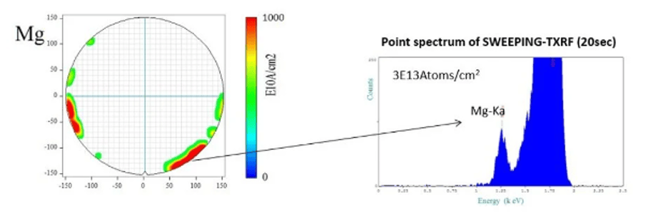
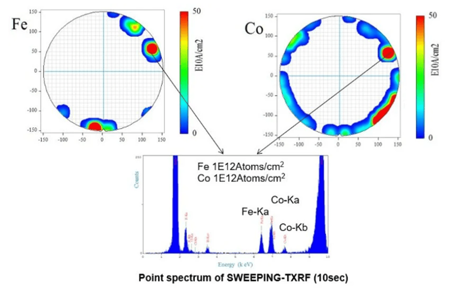
Sample Requirements
- Samples must have flat, polished surfaces (e.g., silicon wafers)
- Compatible wafer sizes: 200 mm and 300 mm
- Surfaces must be free of debris and water droplets
- Surface must be dry and free of particles
- Compatible with materials used in semiconductor processing
TRXF Applications by Industry
Semiconductor
The main application of TXRF is ultra-trace, non-destructive elemental contamination monitoring of semiconductor wafers and thin films.
Techniques That Complement Nanoindentation
Frequently Asked Questions
What is the difference between TXRF and EDXRF?
TXRF (Total Reflection X-ray Fluorescence) uses a grazing incidence X-ray beam, making it highly surface-sensitive and ideal for trace analysis on flat substrates. EDXRF (Energy Dispersive X-ray Fluorescence), in contrast, uses a direct incidence beam and is more suitable for bulk analysis, with less surface sensitivity and typically higher detection limits.
What is the difference between TXRF and conventional XRF?
TXRF differs from conventional XRF in that it employs total external reflection, which significantly reduces background noise and enhances sensitivity to trace elements on the surface. Conventional XRF is better suited for bulk or thick samples and generally does not achieve the same low detection limits for surface contamination.