
What Is Wavelength Dispersive X‑Ray Fluorescence (WDXRF)?
Wavelength Dispersive X-ray Fluorescence (WDXRF) is a non-destructive analysis technique used to measure the elemental composition of a given material. WDXRF testing services do so by measuring the characteristic X-ray fluorescence that is generated when a sample is excited by X-rays. The X-ray fluorescence is measured using a range of high-resolution crystal analyzers.
Thin Film Capability
High-Resolution Analysis
Wide Element Range
Why Use WDXRF?
WDXRF spectroscopy provides rapid and non-destructive quantification of the composition of bulk materials and thin films. It also measures film thickness and impurity levels in thin films. Wavelength Dispersive X‑Ray Fluorescence enables verification of metal film deposition, control over process drift, and identification of contamination that could affect device performance.
Non-Destructive
Rapid and Reliable
Contamination Detection
How WDXRF Works
Wavelength Dispersive X-ray Fluorescence (WDXRF) works by using X-rays to irradiate a sample. This process causes the atoms in the sample to emit fluorescent X-rays. These emitted X-rays have specific wavelengths characteristic of the elements present in the sample. Unlike Energy Dispersive X-ray Fluorescence (EDXRF), WDXRF spectroscopy separates these emitted X-rays’ wavelengths by using crystals to diffract the X-rays. This provides superior spectral resolution to resolve interference from nearby peaks and improve accuracy in complex samples.
The AZX 400 detects and quantifies elemental concentrations by measuring the intensity of characteristic X-rays using automated multi-crystal spectrometers. The instrument is operated under vacuum or purged with helium to enhance sensitivity, particularly for light elements. This allows for the detection of ultra-thin films and trace contamination, even in complex stacks or low-Z materials. Quantification can be performed using known standards or models based on fundamental parameters.
Equipment Used for WDXRF
We use the Rigaku AZX 400 high-resolution WDXRF spectrometer designed for precise, non-destructive elemental analysis. Capable of measuring elements from Be (Z=4) to U (Z=92), it supports sub-ppm detection limits and thin film measurements from ~1 nm to several microns. With advanced automation, a variety of analyzing crystals, and vacuum-controlled sample chambers, it delivers reliable results while optimizing throughput for high-volume semiconductor and materials testing applications.

Rigaku AZX 400
- Measures a variety of sample types: 10–400 mm wafers, coupons, and sputtering targets (up to 30 kg).
- Analytical flexibility for elements from Be to U, ideal for process R&D and low-volume, high-mix environments.
- Core attributes: 4 kW sealed X-ray tube, sequential-type goniometer, primary beam filter.
- Measurement spot sizes: 30, 20, 10, 1, and 0.5 mm diameter.
- Core options: Wafer Loader, SQX (Scan Quant. X) software, CCD Camera.
- Data processing: External PC with MS Windows® OS.
- Software capabilities: Simultaneous film thickness and concentration analysis, Fundamental Parameter software for thin film studies.
Key Differentiators
| Property | WDXRF |
|---|---|
| Element Range | Be (Z=4) to U (Z=92) |
| Detection Limits | Sub-ppm to percent levels |
| Film Thickness Range | ~1 nm to several microns |
| X-ray Tube | 4 kW Rh target |
| Detectors | Scintillation counter for heavy elements, flow proportional counter for light elements |
| Goniometer | Independent θ-2θ with 0.0005° reproducibility |
| Sample Stage | Automated R-theta |
| Diaphragm | 7-position with attenuators |
| Crystal Changer | Automatic, with LiF (200), Ge, PET, RX9, RX25, RX35, RX45, RX61, RX75 |
| Sample Chamber | Vacuum with Automatic Pressure Control |
| Analysis Software | Fundamental Parameters for quantitative analysis |
| Wafer Handling | Automatic transfer of 300 mm wafers from SEMI-compliant FOUP/FOSB |
Strengths
- Thin films & multilayers accuracy.
- Non-destructive analysis.
- Light & heavy elements.
- Ppm to 100% dynamic range.
- Automated, production-ready platform.
- Minimal prep.
- Inline/QA monitoring long-term stability.
- Quantitative analysis without standards.
Limitations
- Lower throughput for quick screening.
- Needs flat and uniform samples.
- Vacuum or a helium atmosphere is not compatible with volatile samples.
- Limited to surface/near-surface layer analysis.
- Large footprint instrument.
Example Outputs
- Elemental Quantification: Tables showing atomic percentages of elements in thin films or coatings for precise composition analysis.
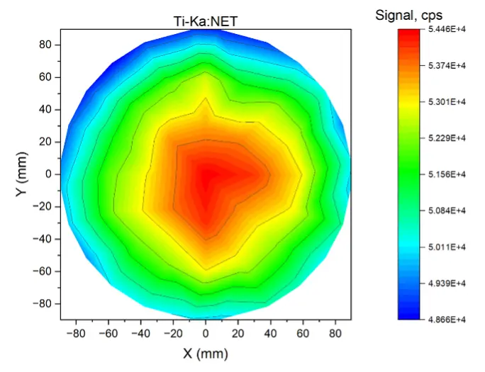
- Film Thickness Profile: Graphical plots across wafers to verify uniformity of sputtered or plated layers.
- Contamination Mapping: Heat maps highlighting trace elements to identify cross-contamination sources in process tools.
- Qualitative Analysis: Intensity vs. angle (2θ) plots with peak identification for verifying material phases and purity.
Sample Requirements
- Flat, solid samples: wafers, films, or coupons.
- No volatile or vacuum-incompatible materials.
- Clean surface, free of particles or debris.
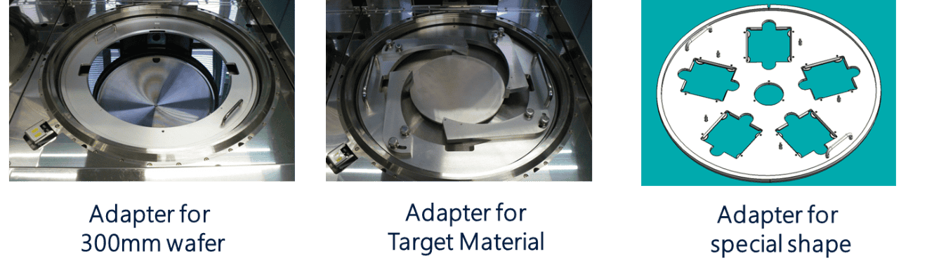
- Maximum size: 400 mm diameter × 50 mm thick, up to 30 kg.
- Adaptable for wafers (up to 300 mm), coupons, sputtering targets, and irregularly shaped samples.
Not sure if your sample qualifies? Talk to our experts for prep guidance and optimal data quality. Other instruments are available to measure powders through Covalent partners.
WDXRF Applications by Industry
Semiconductor Manufacturing
Analyze front-end and back-end wafers, coatings, and interconnects for elemental composition, film thickness, and contamination.
Compound Semiconductors
Measure materials like GaN, SiC, and InP for uniformity, purity, and process control.
Data Storage Media
Verify composition and layer thickness in hard drives, magnetic films, and advanced storage devices.
Solar & Photovoltaics
Assess thin-film solar panels, OLED, and LCD displays for uniformity, contamination, and material quality.
R&D & Advanced Packaging
Support research labs with elemental quantification, thickness mapping, contamination analysis, and phase identification.
Techniques That Complement WDXRF
Why Choose Covalent for Your WDXRF Needs?
Covalent offers advanced WDXRF analysis with the capability of handling full wafers and even larger samples, making it ideal for many samples, including semiconductor and thin-films. At Covalent, we have instruments with high sensitivity and offer a wide range of complementary techniques, allowing for deeper insight.