
What Is Electron Probe Microanalysis (EPMA)?
Electron Probe Microanalysis (EPMA) is a high-precision, quantitative microanalytical technique that measures the elemental composition of solid materials at the micron scale. Also known as Electron Microprobe Analysis or Electron Probe X-ray Microanalysis, EPMA combines imaging and compositional analysis to provide unparalleled accuracy in elemental quantification. The method is valued for its ability to produce highly precise, spatially resolved chemical maps and point analyses.
It uses a focused electron beam to excite X-ray emission from a sample and quantifies the intensities of those characteristic X-rays with wavelength-dispersive spectrometers (WDS).
The key benefit of EPMA is its unique combination of spatial resolution, quantitative accuracy, and sensitivity to light elements (down to Boron with appropriate spectrometers). This makes it ideal for both scientific research and industrial quality assurance.
Micron-Scale Mapping
Wavelength-Dispersive Power
High-Precision Analysis
Why Use EPMA?
EPMA is the method of choice when quantitative accuracy and spatial resolution are both required. Compared to SEM-EDS, EPMA provides far more precise measurements (down to tenths of a weight percentage) and better detection of light elements. It is widely used when compositional standards are available and absolute quantification is needed.
Accurate Quantification
Deeper Material Insight
Confidence in Decisions
How EPMA Works
A finely focused electron beam (typically 1–10 μm in diameter) bombards a polished solid sample, causing atoms to emit characteristic X-rays. Unlike SEM/EDS, which usually employs energy-dispersive detectors, EPMA relies on wavelength-dispersive spectrometers (WDS) with high spectral resolution, enabling separation of overlapping X-ray peaks and very accurate quantification. Multiple spectrometers are mounted on a microprobe, allowing simultaneous collection of different elements.
Quantification is achieved using standards and matrix correction algorithms (e.g., ZAF or φρZ corrections), producing absolute weight percent concentrations with detection limits typically in the 50–100 ppm range.
Equipment Used for EPMA

CAMECA SX100
- Element Range: Boron (B) to Uranium (U).
- Energy Range: 3 keV to 30 keV.
- Current Range: 1 pA to 1 µA.
- Spot-Size: approximately 1 µm to 10 µm.
- Detectors: 4x WDS detectors; 1 SDD EDS detector.
Key Differentiators
Strengths
- Provides highly quantitative results (accuracy better than ±1%) compared to EDS.
- Unlike SEM-EDS, which is semi-quantitative and more dependent on standards and geometry, EPMA routinely uses wavelength-dispersive spectroscopy (WDS) with well-characterized standards.
- Much higher spectral resolution than EDS (resolving overlapping peaks).
- Higher sensitivity for trace elements (down to ~100 ppm in many cases).
- Simultaneous multi-element analysis with multiple spectrometers.
- Detects and quantifies light elements (B, C, N, O, F) when spectrometers are configured.
Limitations
- Requires solid, polished, vacuum-compatible samples (no liquids, powders, or outgassing materials).
- Not suitable for trace analysis below ~50 ppm.
- Interaction volume limits true depth profiling.
- Lower throughput than SEM-EDS due to longer acquisition times and need for standards.
- Conductive coating often required for insulating samples.
Example Outputs
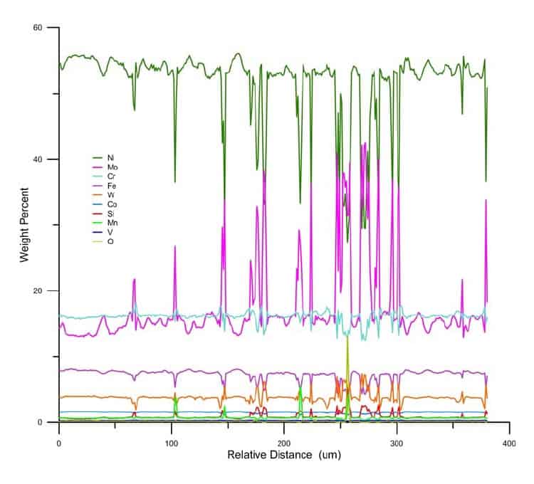
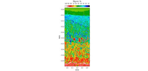
Sample Requirements
- 25–30 mm diameter epoxy mounts or standard thin sections.
- Flat, polished, and conductive coated (usually with C or Au/Pd).
EPMA Applications by Industry
Semiconductor Industry
Mapping dopant distributions in silicon devices.
Energy Materials
Quantifying oxygen and transition-metal ratios in battery cathodes.
Geoscience
Characterizing mineral zoning to interpret thermal histories of rocks.
Aerospace
Compositional verification of high-temperature ceramics.
Techniques That Complement EPMA
Why Choose Covalent for Your EPMA Needs?
Ideal for industries like semiconductors, energy storage, aerospace, and advanced materials, Covalent’s EPMA combines imaging and compositional analysis to reveal detailed elemental distributions and microstructural insights. Their non-destructive technique enables analysis of valuable and complex samples with exceptional accuracy and spatial resolution.
Frequently Asked Questions
What is EPMA used for?
How do EPMA and SEM differ?
SEM focuses on high-resolution imaging of surface features with optional semi-quantitative analysis, while EPMA is optimized for precise quantitative elemental analysis using wavelength-dispersive spectrometers.