
What Is Nanoscale Secondary Ion Mass Spectrometry (NanoSIMS)?
NanoSIMS is a powerful analytical technique designed for ultra-high-resolution elemental and isotopic imaging at the nanometer scale. By visualizing how elements and compounds are distributed within materials or biological samples, researchers can diagnose failures, trace processes, and authenticate materials, driving innovation in fields from semiconductors and medicine to green energy and forensic science.
Trace-Level Sensitivity
Ultra-High Spatial Resolution
Simultaneous Multi-Element Detection
Why Use NanoSIMS?
A key feature of NanoSIMS is its exceptional spatial resolution, capable of imaging features as small as 50 nanometers. This is achieved through a coaxial lens system that positions the ion probe extremely close to the sample surface. The primary ion beam strikes the sample at a perpendicular angle (90°), while the secondary ions are extracted back through the same optical path, minimizing distortions caused by surface topography or shadowing.
NanoSIMS is equipped with up to seven detectors at the mass analyzer’s exit, six of which are movable. This configuration allows for the simultaneous detection of up to seven different ionic species originating from the same sputtered volume. Such parallel detection ensures accurate measurement of isotopic or elemental ratios and enables a direct comparison of their spatial distributions.
The instrument’s mass resolution is also outstanding, with M/ΔM values exceeding 5000. This high mass resolution allows NanoSIMS to distinguish between ions with nearly identical masses, such as 13C14N⁻ (27.000 Da) and 12C15N⁻ (27.006 Da). The use of a double-focusing Mattauch-Herzog-like geometry and optimized transfer optics ensures high transmission efficiency, even at high mass resolution, which is crucial for analyzing small volumes of complex materials.
Unlike time-of-flight SIMS (ToF-SIMS) instruments, NanoSIMS operates in direct current (DC) mode, providing sensitivity that is several orders of magnitude higher and mass resolution that is independent of the spot size. Cs⁺ beams are used for detecting negative ions (e.g., CN⁻) and O⁻ beams for positive ions (e.g., Na⁺). This flexibility allows for the analysis of a wide range of elements, though it does limit which elements can be detected simultaneously.”
Isotopic Ratio Precision
Minimal Topography Effects
Versatile Application Reach
How NanoSIMS Works
The process begins with a fine-focused primary ion beam—typically less than 50 nanometers in diameter—composed of ions such as cesium (Cs⁺) or oxygen (O⁻). This beam is rastered, or systematically scanned, across the surface of a sample. As the primary ions strike each pixel of the sample, they sputter secondary ions from the surface. These secondary ions are then collected and analyzed, allowing NanoSIMS to construct detailed, high-resolution maps of elemental and isotopic distributions.
Equipment Used for NanoSIMS

CAMECA NanoSIMS 50L
- High-resolution mapping: Provides detailed elemental and isotopic imaging at the nanoscale.
- Simultaneous detection: Measures up to seven ionic species from the same sample volume.
- High sensitivity: Continuous Cs+ or O− ion beams enhance detection compared with pulsed systems.
- Precise mass analysis: Double-focusing optics deliver high ion transmission and mass resolution.
- Reduced topographic effects: Compact, co-axial ion optics improve spatial resolution across complex surfaces.
Key Differentiators
- Surface Sensitivity: Extremely high (monolayer sensitivity).
- Mass Range: 1 to >10,000 atomic mass units.
- Molecular Detection: Yes.
- Imaging Capability: Excellent spatial visualization at nanoscale.
- Depth Profiling: Up to a few microns.
- Depth Resolution: ~10 nm.
Strengths
- Exceptional Spatial Resolution: Achieves imaging down to 50 nanometers, enabling detailed nanoscale elemental and isotopic mapping.
- High Mass Resolution: Mass resolution (M/ΔM > 5000) allows discrimination between isotopes and molecular ions with very small mass differences.
- Simultaneous Multi-Element Detection: Up to seven ionic species can be detected at once from the same sputtered volume, ensuring accurate ratio and distribution comparisons.
- Minimized Topography Effects: Coaxial geometry reduces shadowing and topography artifacts, improving data reliability.
- High Sensitivity: DC operational mode provides ppm-level detection limits and sensitivity several orders of magnitude higher than ToF-SIMS, with mass resolution independent of spot size.
- Flexible Element Detection: Positive or negative ion modes accommodate a broad range of elements and isotopes.
- 3D Analysis: Integrates spatial and depth information for full 3D chemical reconstruction.
Limitations
- Element Detection Constraints: Only ions of one polarity can be detected at a time, limiting simultaneous detection of all elements.
- Chemical State Information: Limited.
- Sample Preparation Demands: High spatial resolution and sensitivity require careful sample preparation to avoid artifacts and ensure accuracy.
- Instrument Complexity: Advanced optics and detector systems increase operational complexity and require specialized expertise.
- Limited Throughput: High-resolution mapping and multi-element detection can be time-consuming, especially for large sample areas.
- Destructive Analysis: Applies when performing depth profiling.
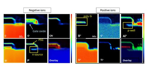
Example Outputs
Sample Requirements
- Metal Samples: A very high-quality metallographic polish is essential to achieve a flat surface and a scratch-free finish, which ensures accurate analysis and minimizes artifacts in the data.
- Biological Samples: Specific protocols must be developed for each experiment to preserve both the structure and the true spatial distribution and abundance of molecules within the sample. Given the operational requirements of the NanoSIMS (ultra-high vacuum), biological samples must be vacuum compatible (volatile free), flat to reduce varying ionization trajectories, and conductive, which can be achieved by sputter coating with Au, Pt, or C. Preparation typically involves fixation using chemical fixation or cryo-fixation, embedding in resin, sectioning into thin slices between 100 nm to 1 μm, and mounting on silicon wafers or slides for analysis.
NanoSIMS Applications by Industry
Semiconductor & Electronics
High‑resolution dopant mapping, contamination detection, and defect localization to ensure device reliability and manufacturing precision.
Biological & Medical
Visualizes nutrient transport, drug uptake, and isotopic tracers in cells and tissues with nanoscale chemical detail.
Green Energy
Characterizes interfaces in batteries, fuel cells, and photovoltaic materials to improve performance, stability, and lifetime.
Materials Science & Catalysts
Reveals nanoscale chemical distributions in alloys, thin films, and catalysts to guide innovation in advanced material design.
Geosciences & Planetary Science
Determines isotopic ratios and trace element compositions in minerals, meteorites, and planetary materials for origin and evolution studies.
Forensics
Identifies trace residues, particulates, and isotopic signatures to authenticate evidence and support investigations with nanoscale precision.
Techniques That Complement Nanoindentation
Why Choose Covalent for Your NanoSIMS Needs?
Covalent provides end-to-end support for NanoSIMS projects, from study design and sample logistics to data interpretation. Our scientists and engineers combine advanced material characterization expertise with clear communication, tailored reporting, and collaborative problem-solving to deliver high-quality, decision-ready insights for your specific application.