
What Is Ultraviolet Photoelectron Spectroscopy (UPS)?
Ultraviolet photoelectron spectroscopy (UPS) is a highly surface-sensitive analytical method that employs ultraviolet light to remove electrons from the surface of a material. It gathers electrons from the Fermi level (if occupied) to the down to states with binding energies near the ultraviolet probe energy. It’s most typically used to calculate the work function (WF) of the target sample surface.
This enables scientists to investigate the electronic structure at the material’s surface.
By measuring the kinetic energy of these ejected electrons (photoelectrons), researchers can obtain valuable information about:
- The structure of the material’s valence band.
- Energies of molecular orbitals.
- The work function of the surface.
This technique provides detailed insights into the material’s electronic characteristics by focusing on the properties of electrons located near the outermost surface region.
Surface Cleaning
High Resolution
Surface Sensitivity
Why Use UPS?
UPS is one of the few means of measuring WF, and for clean samples, often the most accurate. It is non-destructive, so a sample can be measured and then further patterned for device measurement.
There are two common alternatives for WF measurement: XPS and KPFM.
- XPS can be used in place of UPS when:
- UPS is not available, in which case it’s an acceptable though slightly lower resolution technique, or when ultraviolet light is found to alter the chemistry of the sample surface, as is frequently the case with ITO or some polymers.
- KPFM can be used in place of UPS when:
- UPS is not available, in which case it’s an acceptable though slightly lower resolution technique, or for samples that are unstable in vacuum, or for insulating samples that cannot achieve surface charge compensation.
Accurate Work Function
Electronic Structure Insights
Non-Destructive Analysis
How UPS Measurement Works
UPS can be described as a 3-step process, composed of light absorption, photoelectron emission, and photoelectron detection. Ultraviolet light, produced by a He lamp and filtered to the He I line (21.22 eV), is incident on the sample surface. This energy is absorbed by the molecular orbitals at the sample surface, exciting electrons at varying rates. Excited electrons escape their orbitals and may travel in a variety of directions, but a significant portion travels toward the surface and reaches it without inelastic collisions. The electrons that have enough residual energy (after escaping their orbital and reaching their surface) elevate beyond the material surface and enter vacuum are able to get to the detector system. The analyzer splits the incoming electrons by their kinetic energies into differently angled trajectories and captures them in different channels, producing a readout of counts vs kinetic energy.
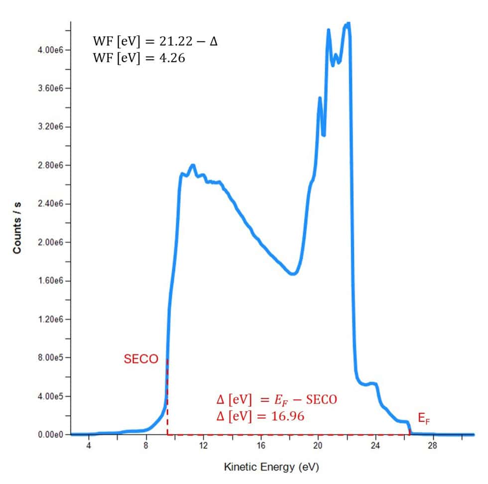
The native output of UPS is a spectrum, showing counts of electrons detected vs. their kinetic energies as measured at the detector. There are multiple transformations to perform on this data, including converting kinetic energy to binding energy, differentiating the data to define cutoff levels for e.g. WF measurements, etc. DOS can be approximated from the data as collected, but accurate modeling requires multiple extra factors to be considered, like (but not limited to) absorption cross-section and inelastic scattering.
Work function, density of states, and band-bending analyses are beyond the scope of this article, but they are covered in some of the linked references.
Equipment Used for UPS

ThermoFisher Nexsa
- Spot Size: 10µm to 400µm.
- Sensitivity: 0.01 atomic % to 0.5 atomic % depending on the element.
- X-ray Source: Monochromated, micro-focused, high-efficiency Al Kα X-ray Anode.
Key Differentiators
The Nexsa surface analysis system can clean the surface using Argon ion clusters ensuring that work function measurements can be done with clean rather than environmentally contaminated surfaces.
Strengths
- UPS is a relatively fast, high-resolution, and high signal-to-noise method of measuring surface electron energies and of calculating WF.
- Covalent’s ThermoFisher Nexsa system is a combination UPS, XPS, and ISS system with built-in depth profiling, charge compensation, and sample tilt control.
- It can combine XPS and UPS to provide a clearer picture of surface chemistry, and utilize ionized Argon to clean or depth profile the surface.
Limitations
- UPS is sensitive to all occupied electron states near the surface (~2 nm) of the material. It is not exclusively sensitive to monolayers, nor is it sensitive to buried materials.
- Sensitivity to occupied states means that it is not able to detect the Fermi level of materials with unoccupied band gaps, and it will detect defect states, trap states, or states from undesired materials such as surface contamination or oxidation. These extra states can lead to confused analysis.
Example Output
Sample Requirements
- Material Compatibility : UPS requires a high vacuum environment, so samples must be stable under those conditions. A typical sample is a flat solid, like a wafer coupon. Insulating surfaces may produce incorrect results due to surface charge accumulation and should be grounded during the measurement if possible. Surface cleanliness is a requirement, so care should be taken in sample handling. Typical lateral sample size is 1×1 cm, and maximum size is 6×6 cm.
- Spatial Resolution: The spatial resolution of the tool is not well characterized. The probe is estimated to be ~2 mm wide. This should be considered a limitation for small feature targeting, and mapping may not be feasible or practical.
- Depth Profiling: Depth profiling is possible with UPS, but requires a very cautious approach, and may not work for many materials. Typically, depth profiling is performed with a monoatomic Argon beam. This effectively removes material at a nms-per-minute pace, but damages and mixes the material during the etch, causing chemical changes, and varying the WF and DOS of the remaining material. Depth profiling may be possible with alternation between monoatomic and cluster argon beam usage, wherein the latter would be used to remove a thin layer of damage and recover a ‘pristine’ surface, but this often requires experimentation.
UPS Applications by Industry
Semiconductor Manufacturing
In-situ UPS in fabrication chambers measures work function and ionization energy at metal/metal and metal/semiconductor junctions, enabling determination of Schottky barrier height and built‑in potential, which directly drive device performance.
Academic Research
UPS is used to study the electronic properties of semiconductor materials and layered structures, including work function, ionization energy, and phenomena such as Schottky junction behavior and Fermi level pinning.
Techniques That Complement UPS
UPS and XPS can be used complementarily to understand the chemical composition, bonding environment, and electronic structure of surface materials.