
What is VPD-ICPMS?
Vapor Phase Decomposition (VPD) coupled with Inductively Coupled Plasma Mass Spectrometry (ICPMS) is a combined sample preparation and analysis technique used to measure ultra-low levels of metallic contamination on wafer surfaces and thin films. The method employs a vapor-phase acid to dissolve surface residues into a droplet, which is subsequently analyzed by ICP-MS for sensitive, multi-element detection. VPD-ICPMS is widely used in semiconductor manufacturing and materials science where contamination at the parts-per-trillion level can impact device performance and yield.
Surface Sensitivity
Enables detection of trace surface of E6-E10 atoms/cm2 for 300mm wafers.
Full wafer coverage
Measures over the full wafers surface. Bevel edge can also be exclusively measured.
Full Elemental Scans
Supports multi-element analysis in a single measurement.
Why use VPD-ICPMS?
- Detects metallic contamination at concentrations far below the capability of other analytical techniques.
- Process R&D: Detects and measures trace contamination sources that contribute to device failure or reduced reliability, supporting tighter process control in semiconductor manufacturing where even minimal contamination can significantly affect yield.
- Process Control: Generates quantitative, reproducible data suitable for statistical process control (SPC) of wafer surface cleanliness.
- Performed in a cleanroom environment minimizing sample contamination risk.
- Compatible with standard wafer formats (200–300 mm). Smaller wafers can also be analyzed using a special holder.
Highest sensitivity
By collecting contamination from the entire wafer surface VPD-ICPMS can provide superior sensitivity for surface metals.
True surface-specific quantification
Only contaminants on the wafer surface and in the native oxide are measured.
Multi-element analysis (from Li to U)
Transition metals and other key contaminates are measured simultaneously.
How VPD-ICPMS Works
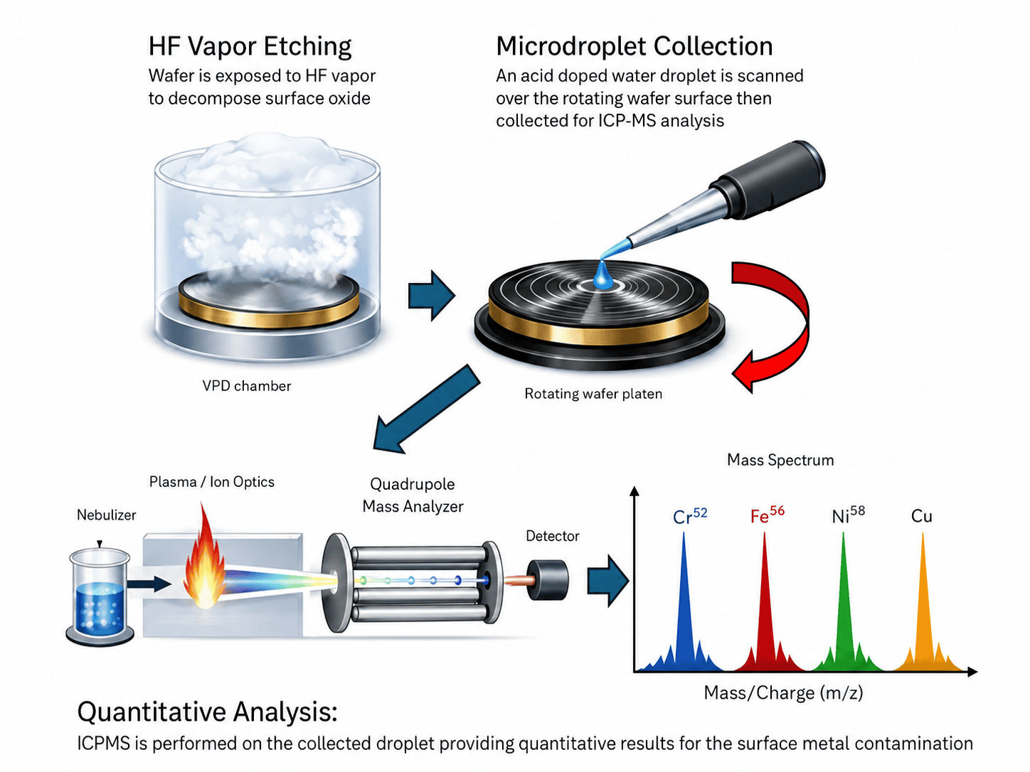
In VPD-ICPMS, the silicon wafer surface is exposed to a controlled vapor of hydrofluoric acid, which decomposes the native silicon dioxide layer and releases metallic contaminants. A small, doped, water droplet is then scanned over the wafer surface by rotating the wafer while the microdroplet is held from above by a pipette. After the full wafer surface is scanned the droplet is collected and introduced into an Inductively Coupled Plasma Mass Spectrometer (ICP-MS). In the ICP-MS, the sample is atomized and ionized at high temperature to generate charged species, which are then introduced into a mass spectrometer. The instrument separates and quantifies these ions based on their mass-to-charge ratio, enabling detection of elements at extremely low concentrations.
Equipment Used for VPD-ICPMS


PerkinElmer NexION® 5000
- Industry-first four-quadrupole design: Full-length Q0+Q1+Universal Cell+Q3 with <0.7 amu resolution for interference removal beyond triple-quad.
- Sub-ppt detection limits: BECs <1 ppt even in hot plasma for ppq-level sensitivity in semiconductor, biomonitoring, and advanced materials.
- Universal Cell with dynamic bandpass tuning: Reactive and collision gas modes for precise elimination of complex polyatomic interferences.
- Maintenance-free plasma system: 34 MHz LumiCoil™ RF generator + OmniRing™ Triple Cone Interface for unmatched matrix tolerance and long-term stability.
Key Differentiators
VPD-ICPMS provides highly sensitive, surface-specific quantification of metallic contaminants at ultra-trace levels relevant to advanced semiconductor processes.
Strengths
- High sensitivity for surface contamination.
- Extremely low detection limits.
- Quantitative multi-element analysis.
- Provides an average value for the entire wafer.
- Established method in semiconductor industry.
Limitations
- Does not distinguish between particulate and plated sources of contamination.
- Single-point measurements are not supported; localized regions, including bevel areas can be analyzed, with detection limits dependent on the area scanned (smaller areas result in reduced sensitivity).
- Typically limited to wafer surfaces; patterned wafers may introduce analytical challenges.
- Involves removal of the surface oxide layer during analysis, limiting the ability to perform repeat surface measurements.
- Analysis of additional elements beyond the standard 41 elements is possible but may require alternative extraction chemistry to remove from the sample surface.
- Requires specialized cleanroom facilities.
- VPD is not intended for bulk material analysis.
Example Outputs
Example output consists of concentration values for elements such as Fe, Cu, Ni, and Zn reported in atoms/cm², typically presented in tabulated form or bar charts.
Example VPD-ICPMS results from a processed 300mm silicon wafer
Element |
| Measured Concentration | Detection Limit E10 Atoms/cm3 |
Aluminum | (Al) | 1.2 | 0.1 |
Antimony | (Sb) | ND | 0.001 |
Arsenic | (As) | 0.6 | 0.2 |
Barium | (Ba) | ND | 0.0008 |
Beryllium | (Be) | ND | 0.1 |
Bismuth | (Bi) | ND | 0.0005 |
Boron | (B ) | 4 | 2 |
Cadmium | (Cd) | ND | 0.002 |
Calcium | (Ca) | 1.2 | 0.1 |
Chromium | (Cr) | 0.1 | 0.03 |
Cobalt | (Co) | ND | 0.03 |
Copper | (Cu) | ND | 0.01 |
Gallium | (Ga) | ND | 0.002 |
Germanium | (Ge) | ND | 0.005 |
Iron | (Fe) | 0.9 | 0.05 |
Lead | (Pb) | ND | 0.002 |
Lithium | (Li) | ND | 0.03 |
Magnesium | (Mg) | ND | 0.05 |
Manganese | (Mn) | 0.05 | 0.01 |
Molybdenum | (Mo) | ND | 0.001 |
Nickel | (Ni) | 0.05 | 0.03 |
Potassium | (K ) | 0.5 | 0.1 |
Sodium | (Na) | ND | 0.1 |
Strontium | (Sr) | ND | 0.005 |
Tin | (Sn) | Nd | 0.01 |
Titanium | (Ti) | ND | 0.03 |
Tungsten | (W ) | ND | 0.0005 |
Vanadium | (V ) | 0.01 | 0.005 |
Zinc | (Zn) | ND | 0.03 |
Zirconium | (Zr) | ND | 0.005 |
ND: Not Detected
Sample Requirements
- Provide clean, contamination-free samples (preferably in wafer carriers).
- Typical sample size: full wafers (200–300 mm) or smaller coupons.
- Avoid handling without gloves in clean environments
- Ship in sealed, clean packaging.
- Specify target elements and detection requirements, if known.
VPD-ICPMS Applications
Monitoring cleaning process effectiveness (RCA, HF last, etc.)
The technique is used to evaluate effectiveness of wafer cleaning steps to remove metallic impurities. By comparing pre- and post-clean VPD extracts, fabs can quantify residual contamination and optimize cleaning chemistries. This is especially important as node sizes shrink and contamination tolerances tighten.
Detection of cross-contamination from process tools
VPD–ICPMS enables identification of trace metal contamination introduced during processing (e.g., from deposition chambers, CMP tools, or handling systems). Elemental fingerprints (e.g., Cu from electroplating, Fe/Ni from stainless steel components) can be traced back to specific toolsets, supporting root-cause failure analysis in semiconductor manufacturing.
Qualification of high-purity chemicals and process materials
The method is applied to assess contamination transferred from ultrapure chemicals, gases, or wafer carriers onto wafer surfaces. After exposure, VPD extraction enables quantification of deposited trace metals. This supports supplier qualification and ensures materials meet stringent semiconductor-grade purity requirements.
Surface contamination mapping and method cross-validation (with TXRF)
VPD–ICPMS provides highly sensitive bulk surface contamination values, while TXRF offers rapid, non-destructive screening and spatial information. The two techniques are often used together: TXRF for mapping and screening, followed by VPD–ICPMS for absolute quantification. This complimentary approach improves confidence in contamination assessment and method validation.
Typical Use Cases (Optics)
VPD–ICPMS can be used to quantify ultra-trace metallic contamination on high-value optical components (e.g., EUV mirrors, laser optics, precision lenses). The VPD step dissolves surface residues without affecting the underlying bulk material, enabling detection of metals such as Fe, Cu, and Na that can degrade optical performance or induce scattering. This is particularly relevant in high-power laser systems and space optics, where even sub-monolayer contamination impacts performance and lifetime.
Techniques That Complement VPD-ICPMS
Offers depth profiling to complement surface-only measurements. Can measure surface contamination under specialized conditions but it is not a survey technique.
Provides non-destructive surface contamination analysis. Detection limits are higher than VPD-ICPMS, but TXRF can map impurities across the wafer surface (with ~1cm spot size).
Used for bulk elemental analysis when surface specificity is not required.
Provides chemical state information alongside elemental detection of surface species, but with ~5e12 atoms/cm2 elemental detection limits.
Enables elemental analysis of surface oxides on localized regions (not full wafers) and can identify surface organics (qualitatively).
Frequently Asked Questions
What detection limits can be achieved?
Detection limits are typically in the 1E6 to 1E10 atoms/cm2 range.
Is the technique destructive?
Yes, the surface oxide layer is removed during analysis.
What sample types are supported?
Primarily silicon wafers. Other wafer types such as SiC, GaAs, etc. can be scanned for surface metals using the same water droplet technique but without the HF vapor decomposition. Metal collection will depend on how tightly the contamination is bound to the wafer surface for non-silicon materials.
How many elements can be detected?
Typically 30 or 41 elements (primarily transition metals) are analyzed. Additional elements can be analyzed but may require modified extraction chemistries.
What industries use VPD-ICPMS?
Primarily semiconductor and electronics industries.