
What Is Atomic Force Microscopy (AFM)?
AFM is a high-sensitive and high-resolution scanning technique that maps materials’ surface topography and properties with sub-nanometer vertical accuracy. As part of the broader Scanning Probe Microscopy (SPM) family, atomic force microscopy techniques stand out for their ability to capture chemical, electrical, mechanical, and magnetic characteristics, often in a single scan.
An AFM tip, typically 2–20 nm in radius, extends from a flexible cantilever and interacts with the sample surface through van der Waals, magnetic, and electrostatic forces. These interactions cause the cantilever to deflect. An optical system measures the deflection by reflecting a laser off the back of the cantilever onto a detector, converting nanoscale interactions into quantitative surface maps.
At Covalent, we tailor our analysis to the scale, complexity, and failure modes across semiconductor, battery, and biomedical industries.
Non‑Destructive
Multimodal
High Resolution
Why Use AFM?
AFM excels when nanoscale behavior drives performance and when other techniques fall short. It enables mapping of vertical deviations, surface interactions, and electrical/chemical domains without damaging sensitive samples.
Material Performance
Unique Resolution
Industry Relevance
How AFM Works
AFM atomic force scanning uses an ultra-sharp probe tip, mounted on a cantilever, across the sample in a raster pattern. The surface forces bend or oscillate the cantilever, and a reflected laser captures these movements in real time.
A feedback loop maintains constant force between the tip and the surface, enabling precise 3D mapping of topographical features at angstrom-level sensitivity.
AFM operates across multiple imaging modes, and each offers unique insights:
- Contact Mode: The tip maintains continuous contact with the surface. Best for rigid samples.
- Tapping Mode (Non-Contact): The tip oscillates near its resonance frequency, minimizing surface damage to soft materials.
- Conductive AFM (C-AFM): Measures current flow through the tip to map nanoscale conductivity.
- Magnetic Force Microscopy (MFM): Detects long-range magnetic interactions, revealing magnetic domains.
- Electrostatic Force Microscopy (EFM): Visualizes and maps surface charge distributions via electrostatic forces.
- Kelvin Probe Force Microscopy (KPFM): Analyzes contact potential difference, estimating surface work function.
- Force Spectroscopy & Force-Volume Mapping: Quantifies adhesion, stiffness, and elastic modulus at specific surface sites.
- Piezo Force Microscopy (PFM): Probes piezoelectric and ferroelectric domains in functional materials.
- Quantitative Nanomechanics (QNM): Measures nanoscale stiffness and modulus with enhanced repeatability across heterogeneous surfaces.
These modes turn AFM from a topography tool into a multimodal platform for material property discovery.
Equipment Used for AFM

Bruker Dimension XR (SCM option), NanoScope V
- AFM platform: Large-sample SPM with PeakForce Tapping for routine atomic-defect and sub-nanometer imaging in air and liquid.
- Nanomechanics: AFM-nDMA for quantitative nanoscale storage/loss modulus over 0.1 Hz–20 kHz, linked to bulk DMA.
- Nanoelectrical: DataCube modes for hyperspectral electrical mapping, giving electrical and mechanical spectra at every pixel.
- Nanoelectrochemistry: PeakForce SECM / EC-AFM for <100 nm-resolution electrochemical imaging with simultaneous topography, electrical, and mechanical contrast.
Key Differentiators
Atomic force microscopes deliver data at a scale where even minor variations in surface can influence functionality or failure.
- Data Outputs: Topography, surface roughness, conductivity, work function, capacitance, modulus, coercivity, adhesion, and charge.
- Sensitivity: Noise floor ~0.05 nm RMS; Vertical range: 0.1 nm to 10 µm.
- Resolution: Lateral (XY): 2–10 nm; Vertical (Z): ~0.1 nm.
- Material Compatibility: Optimized for solids and flat surfaces; some modes operate in liquid environments.
- Depth Profiling: Not standard, but interface mapping is possible via angle-lapping or cross-sectioning.
At Covalent, we extend these outputs into targeted and comparative diagnostics, turning surface data into answers and insights that matter.
Strengths
AFM combines mode versatility, high vertical sensitivity, and nanoscale resolution. Covalent optimizes this capability through strategic execution:
- Application Range: Works across conductive, insulating, soft, fragile, or layered materials.
- Mode Breadth: From force spectroscopy and nanomechanics (QNM) to charge mapping and piezoelectric imaging (PFM), workflows adapt to a wide variety of materials and conditions.
From force spectroscopy to charge mapping, our AFM atomic force workflows are built around the physics of your material and the metrics that define success.
Limitations
AFM is powerful, but context matters:
- Scan Area: Limited to ~90×90 µm.
- Speed: Slower than widefield optical profilometry.
- Sample Geometry: Curved or unstable surfaces pose challenges.
- Tip Lifetime: Artifacts may arise from tip wear or contamination.
- Liquid Imaging: Requires dedicated probes and environments.
We assess feasibility before every scan to ensure the correct method, mode, and output.
Example Outputs
A typical AFM dataset provides multiple co-registered images, each reflecting distinct nanoscale material properties. In the example below, three output channels are displayed: topographic height, adhesion, and peak force TUNA current, captured from a microporous carbon electrode used in hydrogen fuel cells.
The electrode consists of carbon black particles bound by a Teflon-like polymer. While this binder improves mechanical integrity and membrane adhesion, it can reduce through-plane conductivity and lower fuel cell performance.
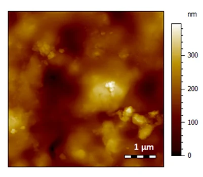
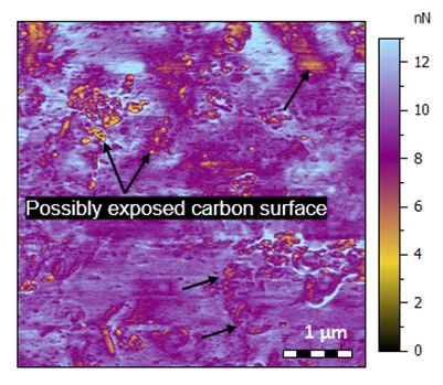
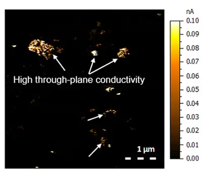
Together, these images provide a multidimensional view of surface structure, mechanical behavior, and electrical performance, enabling rapid imaging, defect localization, and in-depth material diagnostics at the nanoscale.
Sample Requirements
Accurate AFM starts with precise preparation. We guide clients through every step to minimize errors and optimize signal quality.
- Form: Solids are preferred, but liquids are compatible for certain biological applications.
- Stability: Air or Liquid compatible (Example: Water, PBS).
- Size: The ideal sample size is ~1×1 mm. Larger wafers can be mounted directly.
- Prep: May require cleaving, gluing, or fiducial markers for targeting.
Need help preparing your sample? Our team designs mounting protocols based on material type, fixture, and imaging goal.
Atomic Force Microscopy Analysis Applications by Industry
Semiconductor
Sidewall profiling, dopant mapping, gate oxide failure analysis.
Energy Storage
Electrode roughness, degradation tracking, conductive area mapping.
Polymers & Coatings
Phase distribution, film uniformity, stiffness gradients.
Biomedicine
Cell-substrate adhesion, hydrated modulus, nanoscale morphology.
Techniques That Complement Atomic Force Microscopy Analysis
In a broader surface characterization workflow, AFM is often the primary resolution. For deeper insights, it is commonly paired with other techniques. These complementary techniques are chosen based on the resolution needed, material, and failure mode. If you have difficulties choosing the right one, we can always advise on the best combination for the best results.
Why Choose Covalent for Your AFM Needs?
Covalent delivers more than high-resolution AFM images. Our experts tailor each analysis to your sample, using advanced imaging modes, reliable tip protocols, flexible sample preparation, and reference standards to ensure accurate results. We can also integrate AFM findings with techniques such as SEM-EDS, FTIR, and XPS, providing clear, actionable insights into material behavior, processes, and failures.