Failure Analysis
Root cause investigation of material, process, and device failures.
Compositional Analysis
Compositional analysis identifies the chemistry of a material, down to its elements, molecules, and phases. These measurements verify purity and detect impurities before they impact design, production, or compliance.
Metrology Consulting Services
Expert guidance on your metrology strategy and implementation.
Quality Control Testing
The difference between good and exceptional lies in the details. Covalent's Quality Control services delve into those details, providing the assurance that your materials and components consistently uphold the highest benchmarks.
Metallurgical Analysis
Correlating microstructure to processing, properties, and performance of your metallic alloy systems using advanced sample preparation, testing, imaging, and spectroscopy.
Material Verification
Material verification is about knowing exactly what is in your materials. By evaluating materials against the specifications provided, Covalent helps you prevent costly mistakes, failures, and compliance risks.
Contamination Analysis
Identify and resolve particulate, chemical, or organic contaminants that compromise material quality, yield, or device function.
Performance Optimization
Behind every high‑performing product is a series of deliberate choices about materials and process. Covalent partners with you to refine those choices, translating real‑world behavior into smarter tuning, higher yield, and greater reliability.
Surface & Interface Properties
Characterize coatings, thin films, and contamination with advanced material analysis to improve reliability and performance.
Mechanical Testing
Measure mechanical properties with our engineering testing expertise to validate material integrity and ensure optimal performance.
Chemical & Compositional Properties
The elements and structures within a material determine whether a product is safe, reliable, and built to last. Covalent’s chemical composition analysis services give you the clearest possible view of that chemistry.
Metals Testing
Identify and quantify metal composition, microstructure, and mechanical properties to ensure performance, reliability, and compliance for your application.
Coatings Testing
From corrosion resistance to biocompatibility, our testing ensures stronger products and global compliance.
Powder Testing
Covalent delivers specialized powder characterization services, including powder testing for particle size, shape, and flow. We support metal powder testing services and additive manufacturing powder testing to optimize performance in pharma, energy, and industrial applications.
Optical Characterization Testing
Covalent provides precise optical characterization services, delivering critical data on optical properties and thickness for materials, semiconductors, thin films and coatings. Our advanced optical characterization techniques ensure performance, reliability, and compliance.
Polymer & Plastic Analysis
Covalent offers comprehensive polymer & plastic testing lab services for polymer analysis, failure analysis, and quality control. Get fast, actionable data to ensure quality, performance, and compliance.
Atomic Resolution Electron Microscopy (AEM)
Images atoms and maps composition, bonding, and strain.
Differential Phase Contrast
Visualize local electric fields at the nanoscale.
Focused Ion Beam Scanning Electron Microscopy (FIB-SEM)
Combines ion milling and electron imaging for nanoscale analysis.
Nanoprobing
Precession Electron Diffraction (PED)
PED is a TEM-based technique that rotates the electron beam for more precise crystallography at the nanoscale.
Scanning Electron Microscopy (SEM) Analysis
Images surface topography and composition with electrons.
Scanning Transmission Electron Microscopy (STEM)
Provides atomic-scale imaging and spectroscopic mapping.
Transmission Electron Microscopy (TEM)
Images atomic structure, defects, interfaces with sub-nm resolution.
Attenuated Total Reflectance Fourier Transform Infrared Spectroscopy (ATR-FTIR)
Rapid, non-destructive chemical identification.
Auger Electron Spectroscopy (AES)
Measures Auger electrons for high-resolution surface analysis.
Dynamic Secondary Ion Mass Spectrometry (Dynamic SIMS)
Quantifies elements and isotopes with nanometer depth profiling.
Electron Probe Microanalysis (EPMA)
Quantifies elemental composition at the micron scale.
Energy Dispersive X-ray Fluorescence (EDXRF)
Quick, non-destructive material composition & thickness analysis.
Fourier Transform Infrared Spectroscopy (FTIR)
Rapid, non-destructive molecular fingerprinting across materials.
Gas Chromatography-Mass Spectrometry (GC-MS)
Identifies and quantifies small organic molecules in mixtures.
Gel Permeation Chromatography (GPC)
Separates molecules by size to determine polymer properties.
Glow Discharge Optical Emission Spectroscopy (GDOES)
Sputters surfaces to quantify composition & depth-profile layers.
Inductively Coupled Plasma Mass Spectrometry (ICP-MS)
Measures trace elements with high accuracy.
Inductively Coupled Plasma Optical Emission Spectroscopy (ICP-OES)
Quantifies multiple elements at very low concentrations.
Ion Scattering Spectroscopy (ISS)
Identifies elements in the outermost atomic layer.
Nanoscale Secondary Ion Mass Spectrometry (NanoSIMS)
Ultra-high-resolution elemental and isotopic imaging.
Neutron Activation Analysis (NAA)
Quantifies elements via gamma rays from irradiated samples.
Nuclear Magnetic Resonance Spectroscopy (NMR)
Determines molecular structure, composition, and dynamics.
Photo-induced Force Microscopy (PiFM)
Nanoscale chemical characterization & topography at sub-5nm.
Raman Spectroscopy
Measures inelastic photon scattering for chemical identification.
Rutherford Backscattering Spectroscopy (RBS)
Quantifies elemental composition and thin-film thickness.
Time of Flight Secondary Ion Mass Spectroscopy (ToF-SIMS)
Ultra-sensitive surface analysis with chemical imaging & depth profiling.
Total Reflection X-ray Fluorescence (TXRF)
TXRF is a surface sensitive elemental analysis technique used to determine the concentration of trace metal contamination on wafer surfaces.
Ultraviolet Photoelectron Spectroscopy (UPS)
Determines work function and valence electronic structure of surfaces.
Ultraviolet Visible Near Infrared Spectrophotometry (UV-Vis-NIR)
Measures absorbance, reflectance, and transmittance (175–3300 nm).
Wavelength Dispersive X‑Ray Fluorescence (WDXRF)
Non-destructive elemental composition & thin-film analysis.
White Light Interferometry (WLI)
Measures surface topography with sub-nanometer vertical resolution.
X-ray Absorption Spectroscopy (XAS)
Analyzes electronic structure of atoms and molecules.
X-ray Diffraction (XRD)
Non-destructive analysis of crystal phases, lattice, and strain.
X-ray Photoelectron Spectroscopy (XPS)
Measures surface elemental composition and chemical states.
Cathodoluminescence (CL)
Maps bandgap, defects, and strain with SEM correlation.
Digital Optical Microscopy
Rapid, high-resolution imaging of a sample.
Dynamic Light Scattering (DLS)
Quantifies particle size and uniformity in minutes.
Fluorescence Microscopy
Infra-Red (IR) Thermography
Visualizes surface temperatures to reveal defects & hotspots.
Laser Scanning Confocal Microscopy (LSCM)
Non-destructive 3D imaging of sample surfaces.
SNOM-Raman
Maps nanoscale stress and chemistry with 100 nm resolution.
Spectroscopic Ellipsometry (SE)
Measures thin-film thickness & optical properties.
Structured Light Profilometry
Creates precise 3D models without contact or damage.
Capillary Flow Porometry (CFP)
Characterizes through-pores in wettable, permeable materials.
Dye & Pry Testing
Reveals PCB solder joint cracks & defects.
Dynamic Mechanical Analysis (DMA)
Characterizes thermal and mechanical properties of soft materials.
IPC Compliance Testing (IPC Compliance)
Verifies IPC-A-610 quality to reduce defects.
Mechanical Cross-Section Analysis (X-Section)
Uncovers microstructures and defects causing performance issues.
Nano-Scratch Test
Measures lateral/frictional force between tip & sample.
Nanoindentation
Determines mechanical properties including hardness & modulus.
Pendant Drop Surface Tension Measurement
Provides accurate liquid property analysis for surface tension.
Rheology
Evaluates material behavior during processing, storage, and use.
Tap Density
Ratio of sample mass to volume after mechanical tapping.
Tensile Testing
Measures material behavior under axial stretching (tension).
Thermomechanical Analysis (TMA)
Measures material dimension changes with temp, time, or force.
Differential Scanning Calorimetry (DSC)
Quantifies heat flow for material optimization.
Thermogravimetric Analysis (TGA)
Measures material mass changes with temperature or time.
Time-Domain Thermoreflectance (TDTR) Analysis
Time-Domain Thermoreflectance (TDTR) is an optical pump–probe technique used to measure thermal conductivity, thermal boundary conductance, and heat transport properties in thin films deposited on solid substrates.
2D X-Ray Inspection
Delivers clear internal views of complex electronics.
Atomic Force Microscopy (AFM) Analysis
Maps nanoscale topography and material properties with a sharp probe.
Chromatic Confocal Profilometry & 3D Surface Profiling
Fast, non-contact 3D surface measurements.
Gas Adsorption Porosimetry
Characterizes porous materials.
Gas Pycnometry
Fast, precise measurements of true volume, density, and porosity.
Laser Diffraction Particle Size Analysis (LD-PSA)
Analyzes particle sizes by measuring light scattering.
Scanning Acoustic Microscopy (SAM)
Locates internal flaws like cracks, voids, and delamination.
X-ray Computed Tomography (Micro-CT)
Non-contact, non-destructive 2D/3D images at micron scale.
X-ray Reflectometry (XRR)
Optimized scans tailored to each sample for best measurements.
Zeta Potential
Electric potential at the slipping plane of the EDL.
4-Point Probe (4PP) Measurement
Measures sheet resistance and resistivity accurately.
Scanning Capacitance Microscopy (SCM)
Maps charge carrier polarity/distribution in semiconductors.
Surface Free Energy (SFE)
Quantitative insight into surface energy for adhesion and coatings.
Water Contact Angle
Quantitative insight into surface interactions affecting adhesion.
Metallurgical Failure Analysis: Root Cause Investigations
Understanding why materials fail is essential to improving reliability, safety, and performance. This webinar provides an overview of <a…
Beyond the Surface: Next-Generation Scanning Acoustic Microscopy
Scanning Acoustic Microscopy (SAM) is a powerful tool for non-destructive evaluation of internal features such as voids, delamination, and…
SEM vs TEM: Choosing the Right Electron Microscopy Technique for Materials Characterization
A New Octopus Species Revealed with MicroCT
Covalent Expands Wafer-Level Semiconductor Characterization Through Oxford Instruments Collaboration
Covalent today announced a strategic collaboration with Oxford Instruments that expands its semiconductor characterization offering with customer-ready, wafer-level Raman…
Covalent Appoints Damien Fischer as Vice President of Commercial Strategy & Growth
New role strengthens Covalent’s market development, customer growth, and strategic partnership capabilities as the company enters its next stage…
What Really Failed? Understanding Failure in Materials, Components, and Assemblies
This eBook explains how failure analysis helps engineering teams move from visible damage to defensible root cause. Using examples…
Roman Coin Characterization Case Study
This case study presents a multi-technique, fully non-destructive characterization of two Roman coins from the reign of Julian II…
Covalent transforms complex material testing data into clear, actionable insights. From failure analysis to advanced compositional studies, we partner with innovators across industries to accelerate development and optimize performance.
We’re scientists, engineers, and problem-solvers first. Over 70% of us hold PhDs or advanced degrees. Every engagement is led by credentialed experts who combine deep technical knowledge with practical solutions tailored to your toughest challenges.
Trusted by 1,500+ global manufacturers, OEMs, and R&D teams, Covalent builds long-term partnerships that deliver results at scale. Backed by $25M in tools and ISO-accredited methods, we focus on just one thing: data you can act on with confidence.
Join a team that's shaping the future of material insights. At Covalent, you'll work with world-class scientists, cutting-edge technology, and global industry leaders, all while making a measurable impact.
Quality is foundational to our work. Covalent is ISO accredited and operates under a rigorous quality management system. Our processes, data, and results meet internationally recognized standards so you can trust every measurement and insight we deliver.
The Covalent Core Lab provides advanced material characterization and analytical testing performed by Covalent scientists using state-of-the-art instrumentation to deliver fast, reliable results
Covalent Connect provides access to specialized material characterization and testing services through a network of partner laboratories, guided by Covalent scientists for fast, reliable results.
eBook
The best-known method to test the quality of printed circuit boards and their components is Destructive Physical Analysis (DPA). This process yields a comprehensive quality…
Datasheet
Review the Keyence microscopes and profilometers at Covalent! Keyence is a global leader in developing high-resolution optical imaging tools.
eBrief
With so many surface imaging techniques available, it can be a challenge to select the best method for your project. Each technique provides surface data…
Covalent expert team of S/TEM analysts assembled this eBrief to debunk 7 of the most common misunderstandings about modern S/TEM capabilities and applications. They break…
Application Note
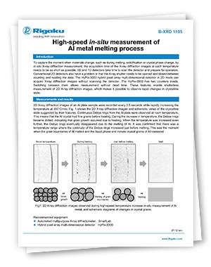
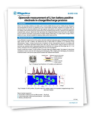
To capture the moment when materials change, such as during melting, solidification or crystal phase change, by in-situ X-ray diffraction measurement, the acquisition time of…
Lithium ion secondary batteries are widely used in small portable devices such as mobile phones. Research and development of lithium ion batteries for use in…