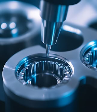
What Is Laser Scanning Confocal Microscopy (LSCM)?
Laser Scanning Confocal Microscopy uses a focused laser to scan the surface of a sample. The confocal pinholes capture only the in-focus surface, thereby enabling the construction of full 3D surface maps. Laser Scanning Confocal Microscopy may also be referred to as VK or VK-X, after the popular Keyence VK (instrument family).
LSCM stands out because it is a non-contact and non-destructive technique that can map the “XY” dimensions and the “Z” height of small features. Laser confocal microscopes combine 2D white-light optical imaging with 3D laser confocal imaging. The Keyence VKX-1100 microscope overlays optimal microscope images with the 3D surface profile for clear imaging of the step heights and surface roughness of small features. Additionally, this instrument is well-suited to examine micron-scale thicknesses of semi-transparent layers and air gaps.

High Resolution
High Resolution
Achieves <1 µm in XY and Z directions.

Fast Scanning
Fast Scanning
Generates 3D maps in minutes.

Material Range
Material Range
Suitable for metals, ceramics, and polymers.
Why Use LSCM?
LSCM is ideal for quick, precise surface profiling when minimal or no sample preparation is required. It delivers high-resolution 3D maps to measure step height, roughness, and film thickness across many material types. Because it’s non-destructive and contact-free, it preserves delicate or polished surfaces while maintaining dimensional accuracy. This makes it essential for semiconductors, materials science, biomedical devices, and precision manufacturing, where surface quality and consistency matter most.

Quick Results
Speeds up surface and defect inspection.

No Prep Needed
Minimizes setup and handling.

Reliable Data
Ensures repeatable, accurate measurements.
Working Principle
For Laser Scanning Confocal Microscopy, a laser source beam is passed through a set of optics with narrow pinholes. These pinholes provide a very shallow depth of field such that only light that is reflected from near the exact focal plane of the final lens will reach the detector.
The microscope captures a series of vertical slices (in z-dimension) to build up a 3-dimensional profile at the illuminated beam spot. By scanning this spot in a raster pattern laterally (in the x-y plane), the system generates an image profile of the sample surface topography.
Nanometer-scale resolution can be achieved, depending on the focusing lens used for the measurement.
Equipment Used for LSCM:
Keyence VKX-1100 Microscope
- Lateral Scan Range: 100 mm x 100 mm.
- Vertical Stage Range: 70 mm.
- Lateral Resolution: < 1 µm.
- Vertical Resolution: < 1 µm (nm-scale possible in some cases).
- Magnification Limit: up to 28,800x.

Key Differentiators
Laser Scanning Confocal Microscopy (LSCM) delivers precise, high-resolution 3D surface mapping without touching or damaging the sample. Covalent’s LSCM stands out for its speed, accuracy, and versatility, capturing detailed topography across metals, ceramics, and polymers with little to no sample prep.
Strengths
- Rapid 3D profile surfaces.
- Non-contact, non-destructive.
- Usually, no sample preparation is required.
- Step heights, profiling small features, surface roughness.
- Measures micron-range features.
- Works with various materials.
Limitations
- For some samples, we need to use Covalent’s alternate optical profilometry or electron microscopy techniques for better results.


Sample Information
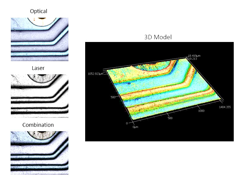
Images captured from the white light source (optical) and laser, as well as the combined image showing how the system captures highly accurate depth contrast as well as the true color of the different pieces of the sample. Pictured at left is a 3D model generated from the height profile of the sample surface; in this image, contrast and color is keyed to height instead of true sample color.
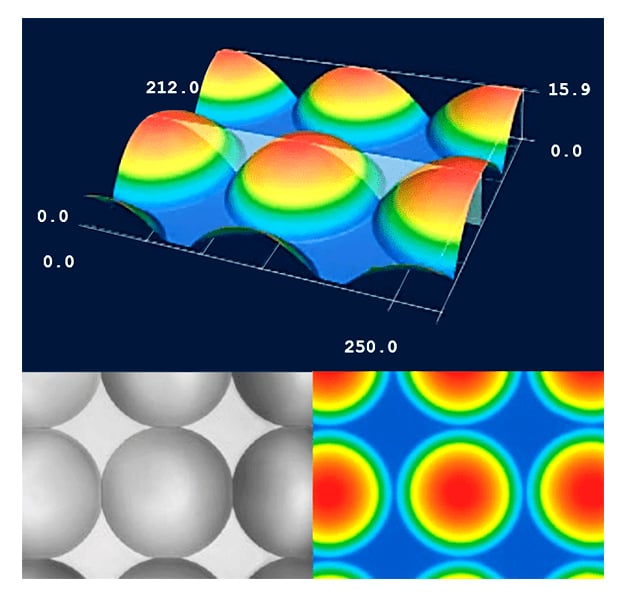
3D models generated from LSCM scans of microlenses, showing radius and circularity.
What we accept:
Samples are typically solids at room temperature. Additional capabilities can allow for heating small samples. If the surface of interest is very transparent and thin, it may be necessary to apply a coating to improve optical reflection at low magnifications.
Use Cases
Semiconductor
Surface inspection of wafers and ICs, quality control, defect examination, deposition measurement, photolithography, and etching.
Microfabricated Devices & Patterned Surfaces
Surface topography, critical dimension measurement, coplanarity, and feature flatness.
Materials Science & Optics
Grain‑structure imaging, sizing, and pattern profiling.
Precision Manufacturing & Metrology
Surface finish, roughness, and dimensioning.
Complementary Techniques
LSCM is a method with various benefits. Depending on your needs, we recommend using it alongside our other techniques for more tailored results.
- AFM (Atomic Force Microscopy): For zooming in on smaller features.
- Chromatic Confocal Profilometry and Structured Light Profilometry: For zooming out to larger features or to map the distribution or density of features.
- SAM (Scanning Acoustic Microscopy) or micro-CT (Micro-Computed Tomography): For a look under the surface.
- SEM (Scanning Electron Microscopy): For an alternate look with improved lateral resolution.
- WLI (White Light Interferometry): For a different view, depending on the surface finish and optical properties.
Atomic Force Microscopy (AFM)
Maps nanoscale topography and material properties with a sharp probe. Explore
Chromatic Confocal Profilometry & 3D Surface Profiling
Fast, non-contact 3D surface measurements. Explore
Scanning Acoustic Microscopy (SAM)
Locates internal flaws like cracks, voids, and delamination. Explore
Scanning Electron Microscopy (SEM)
Images surface topography and composition with electrons. Explore
Structured Light Profilometry
Creates precise 3D models without contact or damage. Explore
White Light Interferometry (WLI)
Measures surface topography with sub-nanometer vertical resolution. Explore
X-ray Computed Tomography (Micro-CT)
Non-contact, non-destructive 2D/3D images at micron scale. Explore
Why Choose Covalent for Your LSCM Needs?
Covalent offers quick turnaround and a broad suite of profilometry tools: LSCM, WLI, AFM, CWL/VR, SEM, SAM, and micro‑CT. These tools are applied by an expert team that selects the right modality and settings for your surface, scale, and tolerance targets.
We deliver quantitative, manufacturing‑ready results: traceable step heights, roughness, stitched 3D maps, and clean data packages. If you prefer a hands‑on approach, you can also schedule a live session to direct regions of interest in real time while we capture the features you care about.
Frequently Asked Questions
Identifying the right test can be complex, but it doesn’t have to be complicated.
Here are some questions we are frequently asked.
What is the vertical resolution in Z?
The vertical resolution in Z is <1 µm, down to 0.1 µm with higher‑NA objectives. For finer vertical resolution, Covalent also offers WLI and AFM.
What is the largest sample area you can measure with this tool?
Confocal laser scanning microscopy is optimal for profiling areas up to ~1 mm², with ~1 µm XY resolution. If needed, larger areas can be stitched or scanned with lower‑NA objectives. For larger areas, measurements are likely better served by other instruments at Covalent.
Is Confocal Laser Scanning Microscopy a good fit for my needs?
Reach out to us at Covalent for a discussion. Tell us a bit about your sample and what you’re trying to learn, and we can provide a free consultation and recommend the right mix of measurements to get you the answers you need.