What Is X-ray Photoelectron Spectroscopy (XPS)?
X-ray Photoelectron Spectroscopy (XPS), also known as Electron Spectroscopy for Chemical Analysis (ESCA), is a surface-sensitive analytical technique that probes the top 70–100 Å of a sample. The technique is based on photoelectrons emitted from atoms on the sample surface after excitation by x-rays, usually Al K-alpha (1487 eV).
The key strength of XPS is its surface sensitivity. The mean free path of the emitted photoelectrons limits the depth from which they can escape and be detected to the top 70 – 100Å of the surface using the typical Take-off-Angle (TOA, measured between the detector and the surface) of 90° and depending on the element from which the electron originated. Changing this TOA to a more grazing angle can reduce the analytical depth. This makes XPS the ideal technique for the analysis of thin films, surface contaminants, and oxidation/corrosion.

Surface-Specific
Analysis
Surface-Specific
Analysis
Provides detailed chemical and elemental information from the top
7–10 nm of a sample, ideal for thin films, coatings, and contamination studies.

Chemical Bonding
Insight
Chemical Bonding
Insight
Determines the bonding states of elements, enabling identification of oxidation, corrosion, and functional groups.

Depth and Angle
Profiling
Depth and Angle
Profiling
Offers depth profiling and
angle-resolved measurements to examine layered materials and surface composition variations.
Why Use XPS?
X-ray Photoelectron Spectroscopy (XPS) is a highly surface-specific technique that provides detailed chemical and elemental information from the top 7–10 nm of a material. It is ideal for analyzing thin films, surface contamination, oxidation, corrosion, and chemical bonding states. XPS enables both depth profiling and angle-resolved analysis, making it indispensable for understanding surface chemistry in industrial and research applications.

High-Resolution Detection
Adjustable spot sizes (10–400 µm) and high spectral resolution for accurate surface characterization.

Advanced Sample Handling
Supports vacuum transfer, angle-tilt mounts, and work function measurements for versatile experiments.

Layered Material Analysis
Argon ion etching enables depth profiling to study composition changes across layers without losing chemical information.

Working Principle
- Elemental Composition:
- XPS collects a survey spectrum over a wide energy range (-10eV to 1350eV) with high signal strength.
- Elements are identified by the detected peaks.
- Peaks are integrated to give the relative atomic percent of each element, normalized to 100%.
- Chemical Bonding Information:
- XPS takes high-resolution spectra focused on specific elements.
- These spectra use settings that enhance spectral resolution.
- Special models are used to fit each peak and determine their exact positions.
- The positions (binding energies) help identify what types of chemical bonds are present, using reference data.
- Depth Profiles:
- XPS can combine measurements with argon ion etching, which slowly removes material from the surface.
- This allows you to see how the composition changes with depth, useful for analyzing layered materials and estimating layer thickness.
- Angle-Resolved Analysis:
- By changing the angle of measurement, XPS can collect information from different depths without removing material.
- This helps estimate the thickness of layers in your sample.
Equipment Used for XPS:
ThermoFisher Scientific Nexsa
- X-ray spot size: 10µ-400 µm.
- Detection limit: 0.1-1%.
- X-ray Source: Monochromated, micro-focused, high-efficiency Al Kα X-ray Anode.
Key Differentiators
Strengths
- Provides chemical bonding information from the top 7-10nm not obtainable with any other technique.
- Capable of analyzing conductors and insulators.
- Compatible with a wide variety of sample types.
- Excellent detection limits (part per thousand for some elements) and spectral resolution.
Limitations
- Does not have ppm detection limits.
- Some sample degradation can occur due to heating from x-ray or flood guns.
- Chemical bonding information is not always possible in-depth profiles due to reduction of sensitive species by argon ion sputtering.
- Not suited to very rough samples (Ra~0.5µm).


Unsure Whether XPS Is Right for You?
Covalent’s mission is to level the playing field and ensure that clients of all backgrounds have access to data generated accurately. Get in touch and we’ll help create a solution for your specific needs.
Sample Information
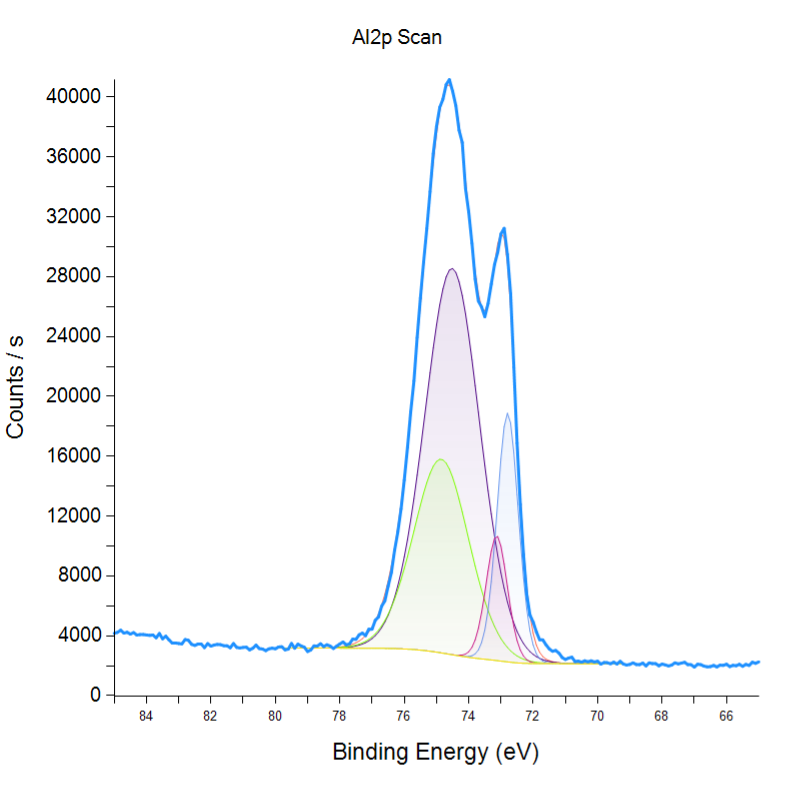
High resolution Al2p spectrum acquired from aluminum foil, peak deconvoluted to separate metal versus oxide. Data can be used to calculate oxide thickness, or 57Â.
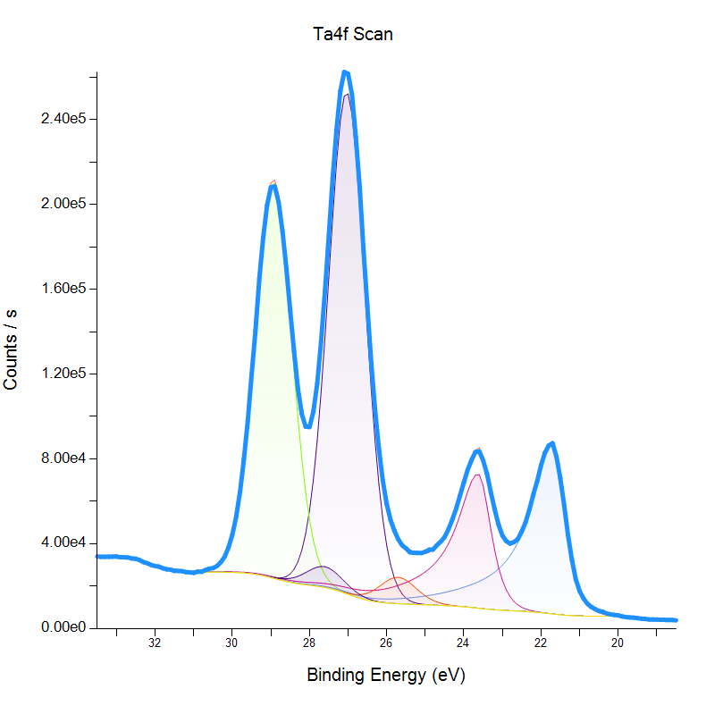
High resolution Ta4f spectrum showing different oxidation states; peak deconvoluted to separate metal versus oxides and suboxides.
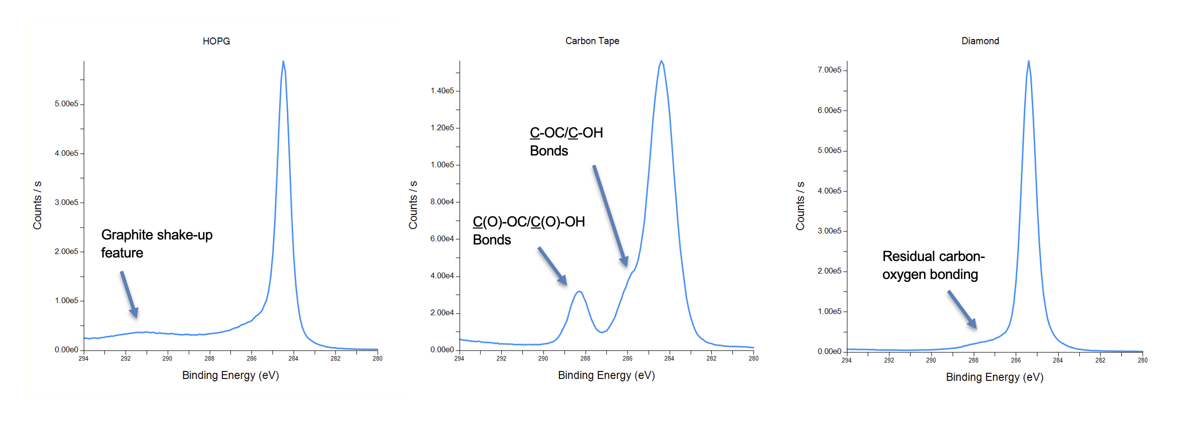
High-resolution C1s spectra showing different forms of carbon: HOPG, diamond, and organic carbon tape
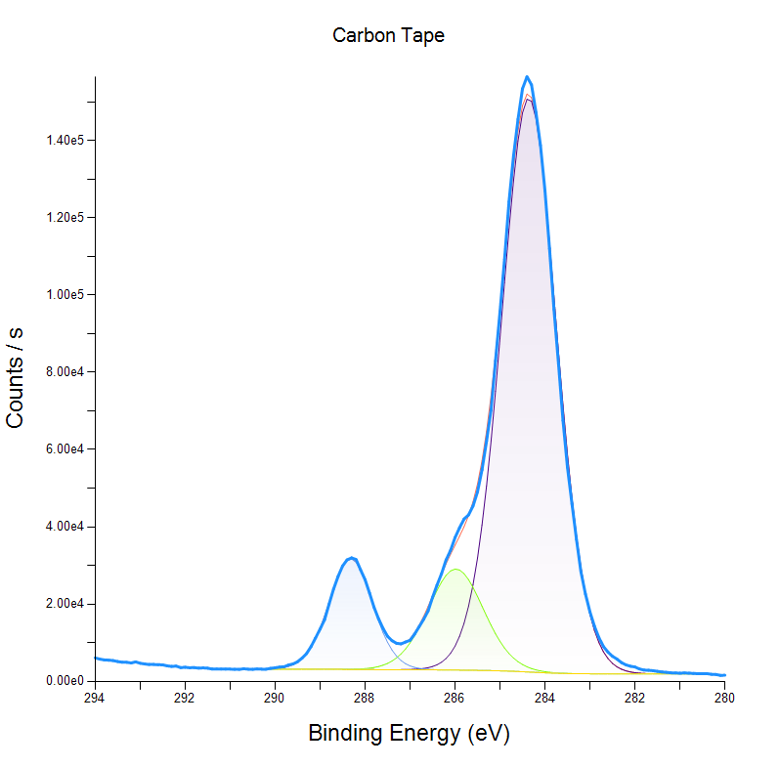
Peak deconvolution of carbon tape C1s high-resolution spectrum showing binding energies and quantitation of different carbon bonding present; indicative of a polyester adhesive
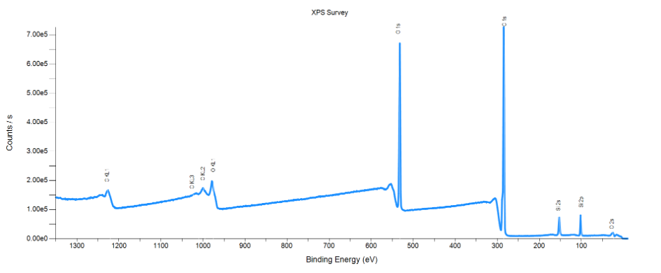
Survey spectrum of carbon tape showing carbon, oxygen and silicon for quantitation of elements detected and to identify contaminants, such as silicon
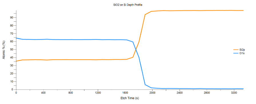
Depth profile of SiO2 on Si used to determine argon ion etch rate based on known thickness and etch time
What we accept:
XPS can analyze any sample compatible with an Ultra-High Vacuum (10-9 mbar) including polymers, powders, cured adhesives, liquid residues, fibers, viscous oil and gels, and any other solid sample.
- Solid phase.
- Stable under ultra-high vacuum conditions.
- Max dimensions: 60 mm (L) x 60 mm (W) x 20 mm (T).
- Flatter topographies improve signal detection.
- For Powder Samples: 5-10 mg is sufficient (as long as it can cover 0.5 cm x 0.5 cm of foil or Cu tape).
Use Cases
XPS is trusted across industries where surface chemistry defines performance:

Semiconductor & Microelectronics
XPS detects surface contamination, and checks oxidation states that could affect device yield. XPS can measure material work functions, critical for semiconductor performance. Depth profiling verifies thin-film chemistry and reveals interlayer diffusion in multilayer stacks.
Aerospace & Defense
XPS identifies oxidation, corrosion, and contaminants on metals and coatings. It validates surface treatments and supports failure analysis of mission-critical parts, such as delaminations.

Energy & Battery Technology
XPS analyzes electrode surfaces, SEI layers, and catalyst coatings for surface contamination and oxidation states, especially effective when paired with inert gas/vacuum transfer directly into instrument.
Polymers / Coatings / Adhesives
XPS detects contamination, chemical variations, and surface treatments on polymer and coating surfaces. It supports adhesion studies and failure analysis, such as delaminations and discolorations.

Medical Devices & Biotech
XPS verifies surface cleanliness, functionalization, and bioactive coatings and surface treatments. It helps detect residues and ensure material compatibility for regulated applications.

Automotive & Industrial Manufacturing
XPS identifies corrosion products, contaminants, and wear-related chemistry. It verifies pre-coat surface quality and supports root-cause investigations.

Environmental & Catalysis Research
XPS determines oxidation states and surface species on catalysts and environmental samples. It aids in evaluating reaction mechanisms and material degradation.
Complementary Techniques
- Auger Electron Spectroscopy (AES): Similar to XPS but making use of the Auger electron transition, initiated by electrons and not x-rays, capable of smaller (~1µm) spot sizes; best applied to depth profiling experiments. Provides limited chemical information. Similar detection limits. Not able to analyze non-conductive samples.
- Time-of-Flight Secondary Ion Mass Spectrometry (ToF-SIMS): Uses different metal ion guns to etch the sample surface, generating ions which are passed to a mass spectrometer to determine mass of ions, which are then used to identify molecular fragments. Species and molecular structures can be identified from the molecular fragments. Data can be very complicated but can provide detailed chemical information. Part per million detection limits.
Auger Electron Spectroscopy (AES)
Measures Auger electrons for high-resolution surface analysis. Explore
Time of Flight Secondary Ion Mass Spectroscopy (ToF-SIMS)
Ultra-sensitive surface analysis with chemical imaging & depth profiling. Explore
Why Choose Covalent for Your XPS Needs?
Frequently Asked Questions
Identifying the right test can be complex, but it doesn’t have to be complicated.
Here are some questions we are frequently asked.
How do the accessories help me do different XPS experiments?
The different XPS accessories allow for a more varied array of XPS experiments, such as air-free transfer (vacuum transfer vessel), angle-resolved analysis, and work function measurements.
Why is having experienced XPS scientists important for understanding my results?
An experienced XPS scientist has knowledge beyond what is available in literature searches, and can quickly distinguish a real peak for an element of interest from an overlap with a secondary peak of another element. An experienced XPS scientist is also skilled in designing specialized experiments to obtain the required information.
What types of information can XPS provide about my sample?
XPS provides elemental composition, chemical bonding and oxidation state information for the near-surface region of a sample, with sensitivity ranging from a few nanometers at the surface to several tens of nanometers using depth profiling or angle-resolved measurements.
How should I prepare my sample for XPS to ensure reliable results?
The recommended method for sample preparation is:
- Avoid contact of any kind with the region of interest.
- Loosely wrap the sample in aluminum foil and secure using double sided tape to the bottom of a rigid container.
- Secure the sample to the bottom of a rigid container with the surface of interest facing up.
What is the analysis depth and spatial resolution of XPS?
- XPS analyzes the top 7-10nm of a surface.
- Spot sizes range from 10 to 400µm (elliptical) and can be adjusted in increments of 5µm.
What is the maximum sample size?
The maximum sample size is 60mm x 60mm x 20mm with a height difference of less than 10mm.

Resources