
Techniques
High‑resolution material data from the right techniques, applied by experts who know what it means for your product.
4-Point Probe (4PP) Measurement
Measures sheet resistance and resistivity accurately. Explore
Atomic Force Microscopy (AFM)
Maps nanoscale topography and material properties with a sharp probe. Explore
Atomic Resolution Electron Microscopy (AEM)
Images atoms and maps composition, bonding, and strain. Explore
Attenuated Total Reflectance Fourier Transform Infrared Spectroscopy (ATR-FTIR)
Rapid, non-destructive chemical identification. Explore
Auger Electron Spectroscopy (AES)
Measures Auger electrons for high-resolution surface analysis. Explore
Capillary Flow Porometry (CFP)
Characterizes through-pores in wettable, permeable materials. Explore
Cathodoluminescence (CL)
Maps bandgap, defects, and strain with SEM correlation. Explore
Chromatic Confocal Profilometry & 3D Surface Profiling
Fast, non-contact 3D surface measurements. Explore
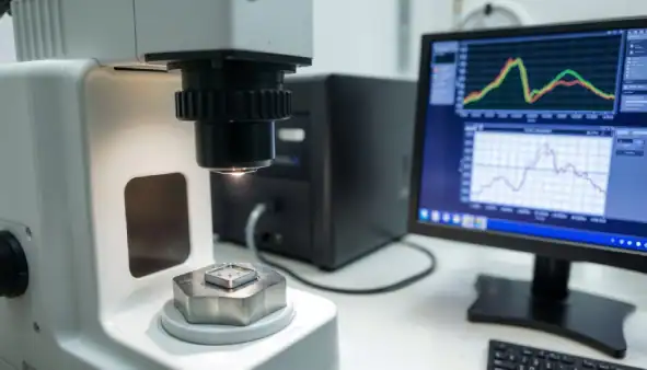
Differential Scanning Calorimetry (DSC)
Quantifies heat flow for material optimization. Explore
Dynamic Light Scattering (DLS)
Quantifies particle size and uniformity in minutes. Explore
Dynamic Mechanical Analysis (DMA)
Characterizes thermal and mechanical properties of soft materials. Explore
Dynamic Secondary Ion Mass Spectrometry (Dynamic SIMS)
Quantifies elements and isotopes with nanometer depth profiling. Explore
Electron Probe Microanalysis (EPMA)
Quantifies elemental composition at the micron scale. Explore
Energy Dispersive X-ray Fluorescence (EDXRF)
Quick, non-destructive material composition & thickness analysis. Explore
Focused Ion Beam Scanning Electron Microscopy (FIB-SEM)
Combines ion milling and electron imaging for nanoscale analysis. Explore
Fourier Transform Infrared Spectroscopy (FTIR)
Rapid, non-destructive molecular fingerprinting across materials. Explore
Gas Chromatography-Mass Spectrometry (GC-MS)
Identifies and quantifies small organic molecules in mixtures. Explore
Gas Pycnometry
Fast, precise measurements of true volume, density, and porosity. Explore
Gel Permeation Chromatography (GPC)
Separates molecules by size to determine polymer properties. Explore
Glow Discharge Optical Emission Spectroscopy (GDOES)
Sputters surfaces to quantify composition & depth-profile layers. Explore
Inductively Coupled Plasma Mass Spectrometry (ICP-MS)
Measures trace elements with high accuracy. Explore
Inductively Coupled Plasma Optical Emission Spectroscopy (ICP-OES)
Quantifies multiple elements at very low concentrations. Explore
Infra-Red (IR) Thermography
Visualizes surface temperatures to reveal defects & hotspots. Explore
Ion Scattering Spectroscopy (ISS)
Identifies elements in the outermost atomic layer. Explore
IPC Compliance Testing (IPC Compliance)
Verifies IPC-A-610 quality to reduce defects. Explore
Laser Diffraction Particle Size Analysis (LD-PSA)
Analyzes particle sizes by measuring light scattering. Explore
Laser Scanning Confocal Microscopy (LSCM)
Non-destructive 3D imaging of sample surfaces. Explore
Mechanical Cross-Section Analysis (X-Section)
Uncovers microstructures and defects causing performance issues. Explore
Nanoscale Secondary Ion Mass Spectrometry (NanoSIMS)
Ultra-high-resolution elemental and isotopic imaging. Explore
Neutron Activation Analysis (NAA)
Quantifies elements via gamma rays from irradiated samples. Explore
Nuclear Magnetic Resonance Spectroscopy (NMR)
Determines molecular structure, composition, and dynamics. Explore
Pendant Drop Surface Tension Measurement
Provides accurate liquid property analysis for surface tension. Explore
Photo-induced Force Microscopy (PiFM)
Nanoscale chemical characterization & topography at sub-5nm. Explore
Precession Electron Diffraction (PED)
PED is a TEM-based technique that rotates the electron beam for more precise crystallography at the nanoscale. Explore
Raman Spectroscopy
Measures inelastic photon scattering for chemical identification. Explore
Rutherford Backscattering Spectroscopy (RBS)
Quantifies elemental composition and thin-film thickness. Explore
Scanning Acoustic Microscopy (SAM)
Locates internal flaws like cracks, voids, and delamination. Explore
Scanning Capacitance Microscopy (SCM)
Maps charge carrier polarity/distribution in semiconductors. Explore
Scanning Electron Microscopy (SEM)
Images surface topography and composition with electrons. Explore
Scanning Transmission Electron Microscopy (STEM)
Provides atomic-scale imaging and spectroscopic mapping. Explore
Spectroscopic Ellipsometry (SE)
Measures thin-film thickness & optical properties. Explore
Structured Light Profilometry
Creates precise 3D models without contact or damage. Explore
Surface Free Energy (SFE)
Quantitative insight into surface energy for adhesion and coatings. Explore
Thermogravimetric Analysis (TGA)
Measures material mass changes with temperature or time. Explore
Thermomechanical Analysis (TMA)
Measures material dimension changes with temp, time, or force. Explore
Time of Flight Secondary Ion Mass Spectroscopy (ToF-SIMS)
Ultra-sensitive surface analysis with chemical imaging & depth profiling. Explore
Transmission Electron Microscopy (TEM)
Images atomic structure, defects, interfaces with sub-nm resolution. Explore
Ultraviolet Photoelectron Spectroscopy (UPS)
Determines work function and valence electronic structure of surfaces. Explore
Ultraviolet Visible Near Infrared Spectrophotometry (UV-Vis-NIR)
Measures absorbance, reflectance, and transmittance (175–3300 nm). Explore
Water Contact Angle
Quantitative insight into surface interactions affecting adhesion. Explore
Wavelength Dispersive X‑Ray Fluorescence (WDXRF)
Non-destructive elemental composition & thin-film analysis. Explore
White Light Interferometry (WLI)
Measures surface topography with sub-nanometer vertical resolution. Explore
X-ray Absorption Spectroscopy (XAS)
Analyzes electronic structure of atoms and molecules. Explore
X-ray Computed Tomography (Micro-CT)
Non-contact, non-destructive 2D/3D images at micron scale. Explore
X-ray Diffraction (XRD)
Non-destructive analysis of crystal phases, lattice, and strain. Explore
X-ray Photoelectron Spectroscopy (XPS)
Measures surface elemental composition and chemical states. Explore
X-ray Reflectometry (XRR)
Optimized scans tailored to each sample for best measurements. Explore
