What Is Scanning Transmission Electron Microscopy (STEM)?
Scanning Transmission Electron Microscopy (STEM) is a hybrid electron microscopy technique that combines the advantages of SEM and TEM. Unlike conventional TEM, the electron beam is focused on a sub-nanometer-sized probe and scanned across the sample to form a STEM image.

Atomic Resolution
Atomic Resolution
Visualize materials at the
sub-angstrom scale, revealing crystal defects, grain boundaries, and interfaces with unmatched clarity.

Chemical Precision
Chemical Precision
Leverage EDS and EELS coupling to map elemental composition and bonding states with nanometer accuracy.

Z-Contrast Imaging
Z-Contrast Imaging
High-Angle Annular Dark Field (HAADF) STEM provides exceptional Z-contrast, ideal for distinguishing layers with varying atomic numbers.
Why Use STEM?
STEM is useful for atomic-scale imaging, as STEM images can provide information on layer thickness, investigate defects and interfaces, provide grain boundary information, and provide Z-contrast imaging.
While TEM and STEM can be used for atomic-scale imaging, STEM has an advantage when imaging samples containing different atomic numbers. For EDS/EELS analysis, STEM mode provides precise beam control, making it a better technique for this case.

Defect and Interface Insight
Pinpoint dislocations, grain boundaries, and hidden defects that impact material and device reliability.

Layer Thickness and Composition Control
Accurately determine nanometer‑scale layer structures and verify chemical integrity across stacks and coatings.

Superior Failure Analysis
Isolate root causes of performance issues; STEM provides detail at the atomic level to guide corrective action.
Working Principle
The raster scanning of the electron probe in STEM makes it suitable for coupling with Energy-Dispersive X-ray Spectroscopy (EDS) and Electron Energy Loss Spectroscopy (EELS). Additionally, the resolution of STEM is determined by the diameter of the probe, making it a powerful tool for structural and spectroscopic mapping of materials at the atomic level.
Equipment Used for STEM:
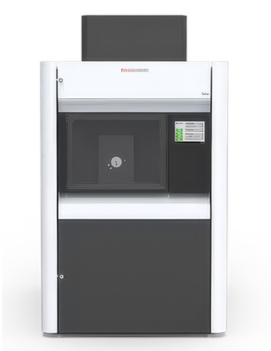
Thermo Scientific Talos F200X G2 TEM/STEM
- Resolution: ≤0.10 nm HRTEM, ≤0.14 nm STEM.
- Chemistry: 4-SDD Super-X EDS for fast 2D/3D mapping.
- EELS: ≤0.3 eV energy resolution (X-CFEG).
- Automation: Velox software for repeatable workflows.
- Versatility: Supports in situ and automated large-area analysis.
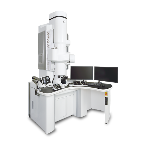
JEOL JEM-F200 Multi-Purpose TEM
- Platform: 200 kV FEG TEM/STEM.
- Analytical: Dual large-area SDD EDS for high-sensitivity mapping.
- EELS: ~0.3 eV energy resolution (cold FEG option).
- Flexibility: Rapid switching between TEM, STEM, EDS, EELS.
- Applications: Ideal for semiconductors, batteries, advanced materials.
Key Differentiators
While both TEM and STEM deliver atomic‑scale insights, each has its own strengths and trade‑offs. Understanding their differences helps in choosing the right technique for specific materials and analytical goals.
Strengths
- Covalent has a cold FEG TEM, which has better EELS energy resolution.
- Precise control of the beam in STEM is very helpful for collecting EDS/EELS.
- STEM provides exceptionally good
Z-contrast imaging, which is a much better way to visualize the layers when they have different average atomic numbers. - STEM is the chosen technique for customers interested in dislocation analysis or chemical composition information.
Limitations
- Expensive tools.
- Destructive technique.
- Elaborate sample preparation.
- Beam-sensitive materials and biological samples are not suited.
- Information comes from a small portion of the sample; multiple samples are needed for statistical analysis.


Unsure Whether STEM Is Right for You?
Get clarity on atomic‑scale imaging and analysis needs. Speak with our experts and explore how STEM can accelerate your research.
Sample Information
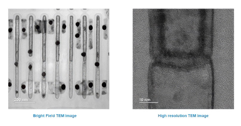
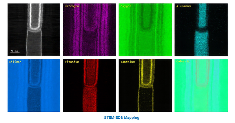
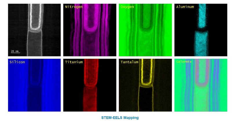
This image exemplifies a Toshiba chip, where a STEM lamella is prepared to understand the structure's layout. TEM, STEM/EDS/EELS data is provided, where STEM images clearly show the Z-contrast information that is missing in the TEM images. EDS and EELS data are provided, showing the 2-D distribution of the elemental composition. EDS and EELS are complementary techniques, and we can choose one or the other depending on the elements of interest and the resolution needed. EELS usually has better resolution than EDS.
What we accept:
- Thin transparent lamella with a thickness below 100 nm.
- Electron transparency.
- For a 2 mm sample size, the elemental composition has to be at least 1 at.% to be detected by EDS or EELS.
- Samples should be conductive for lamella preparation.
Use Cases

Semiconductor
- Used for thin film analysis, defect characterization, and material interfaces.
- Used for nanometer-scale wafer defect analysis to determine which part of the layer stack the defect originates from and its composition using STEM/EDS or STEM/EELS.

Consumer Electronics
Used for thin film analysis, root cause identification of defects, and interface quality at the atomic level.

Defense & Aerospace
Atomic resolution of grain boundaries and precipitates, interface reactions at the nanoscale for coatings.
Battery Research
Used for electrode morphology, degradation mechanisms, and elemental mapping.

Failure Analysis
Used for defect localization, structure and interfaces, and cross-sectional imaging.
Complementary Techniques
- Atom Probe Tomography (APT): Provides 3D atomic mapping with chemical information and complements STEM for atomic-scale analysis in 3D.
- Convergent Beam Electron Diffraction (CBED): Provides local symmetry and strain information.
- Ellipsometry (Ellipsometry): Measures thickness and optical properties of thin films and can be used in a complementary manner with STEM.
- Electron Microscope-Based Techniques (EDS, EELS): Provide chemical information.
- Scanning Electron Microscopy or Cross-Section Scanning Electron Microscopy (SEM): Provides a larger field of view to locate features of interest for STEM analysis.
- Secondary Ion Mass Spectrometry (SIMS): Provides trace elemental analysis that is not possible by STEM/EDS or EELS when the composition is below the detection limit.
- Selected Area Electron Diffraction (SAED) and Nano-Beam Diffraction (NBD): Provide crystallographic information.
- X-Ray Photoelectron Spectroscopy (XPS): Provides surface chemistry and oxidation states of the elements, offering complementary analysis to the elemental information from STEM/EDS or EELS.
Dynamic Secondary Ion Mass Spectrometry (Dynamic SIMS)
Quantifies elements and isotopes with nanometer depth profiling. Explore
X-ray Photoelectron Spectroscopy (XPS)
Measures surface elemental composition and chemical states. Explore
Why Choose Covalent for Your STEM Needs?
Our team at Covalent has experience analyzing samples from various industries. We use high-end STEM tools with sub-nanometer resolution. Our team can provide high-quality data within 2-3 days TAT, sometimes less than 24 hours.
Frequently Asked Questions
Identifying the right test or analysis can be complex, but it doesn’t have to be complicated.
Here are some questions we are frequently asked.
How does Scanning Transmission Electron Microscopy (STEM) compare to Transmission Electron Microscopy (TEM)?
STEM provides Z-contrast imaging; the higher the Z, the brighter the contrast in the image. STEM is a scanning mode technique that has better control over the beam for collecting chemical information.
What is the role of EDS and EELS in STEM analysis?
EELS can be used to understand the elemental composition of materials, bonding information, and the oxidation state.
Can STEM be used to analyze both conductive and non-conductive materials?
Yes, STEM can be used to analyze both conductive and non-conductive materials.
What types of microscopy techniques are used in STEM for elemental mapping?
EDS and EELS.
Can STEM provide elemental mapping?
Yes, by using EDS or EELS.
What is HAADF in STEM?
High-Angle Annular Dark Field imaging.

Resources