What Is a 2D X-Ray?
2D X-ray inspection is a non-destructive failure analysis method that captures hidden faults in the PCBs and BGA solder joints.
Key benefit:
It offers rapid defect detection in PCB X-ray inspection and BGA X-ray inspection, catching hidden failures such as voids, cracks, or Head in Pillow defects without destructive cross-sectioning.

Fast and Non-destructive
Fast and Non-destructive
Quickly identifies hidden defects and Head-in-Pillow failures without cutting or damaging samples.

High Clarity
High Clarity
Reveals fine issues in multilayer PCBs and BGAs, providing detailed defect localization for quality assurance.

Efficient Inspection
Efficient Inspection
Ideal for routine PCB and BGA inspections in production environments.
Why Use 2D X-Ray Imaging?
2D X-ray inspection is a fast, non-destructive approach that adds depth perception for exposing hidden defects in modern electronics. It delivers high-resolution insights into solder voids, cracks, and interconnect failures. It supports high-throughput PCBA inspection services without damaging or altering fragile assemblies. It is well-suited for multilayer PCBs, BGAs, and high-density packaging.

Improved Defect Visibility
Pinpoint and quantify crystalline phases to confirm purity, detect impurities, and verify processing outcomes.

High-Magnification and Resolution
Captures micron-level features with up to 68,000× total magnification for precise analysis.

Flexible Energy Range
Operates from 30–160 kV and accommodates samples up to
740 × 580 mm, supporting diverse materials and assemblies.
Covalent’s Capabilities Offer 2D X‑Ray
Inspection for Non‑Destructive Internal
Defect Detection

Working Principle
- An X-ray source projects radiation through the sample at multiple tilt angles.
- By tilting or rotating the sample, the system captures angled projections that reduce feature overlap and reveal clearer details of hidden structures.
- Denser regions absorb more radiation (appearing darker), while lighter regions allow greater transmission.
- Highly effective for PCB X-ray inspection and BGA X-ray inspection, where hidden solder or interconnect defects can be resolved.
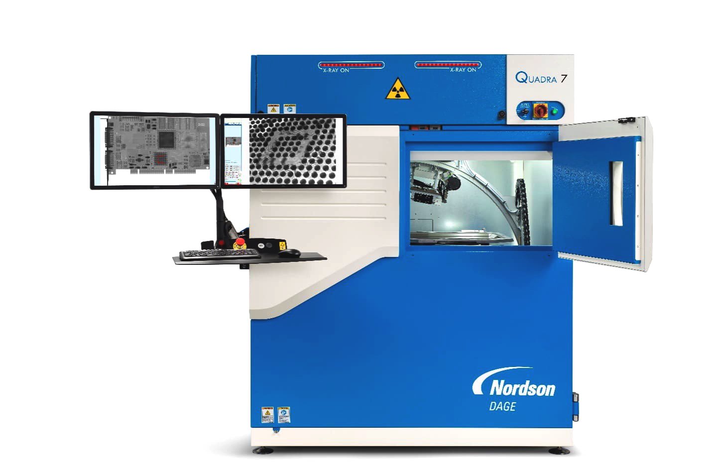
Equipment Used for 2D X-Ray Inspection:
Nordson Dage Quadra 7
- Energy output: up to 160 kV.
- 100 nm feature recognition.
- 7 MP flat panel digital detector.
- 30 fps framerate.
- 0–70° oblique angle view.
- Inspection area: 20 × 17.5 in.
- Geometric magnification: UP TO 2.5 kx.
- Total magnification: up to 68,000x.
- Dosage control for X-ray sensitive samples.
- High Dynamic Range (HDR) enhancement software.
Key Differentiators
- Analytical Depth:
- Captures 2D radiographs with contrast from material density and thickness variations, enabling detection of hidden voids, cracks, and misalignments without destructive cross-sectioning.
- Detection Limits:
- 30–250kV energy range (in-house).
- Up to 250kV with partners.
- Resolution suitable for micro-voids and interconnect failures in BGA X-ray assemblies.
- Material Compatibility:
- Metals, ceramics, polymers, composites.
- Specialized for PCBA inspection services and multilayer boards.
- Sample Size and Weight:
- Up to ~740 × 580 mm and 5 kg.
- Effective area: ~510 × 445 mm.
Strengths
- Rapid throughput for PCB X-ray inspection.
- Flexible dosage allows safe imaging of sensitive devices.
Limitations
- Projection-Only Imaging: Produces flat radiographs, limiting depth analysis compared to Micro-CT scanning.
- Penetration Limits: Very dense or thick samples can reduce image clarity, introduce artifacts, or obscure fine details.


Unsure Whether 2D X-Ray Inspection Is Right for You?
Learn how 2D X-ray inspection can reveal hidden defects in PCBs and BGAs, helping you make faster, more confident electronics decisions.
Sample Information
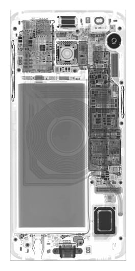
2D X-ray Radiograph of a conventional smartphone, illuminating the interior features and components without disassembly or destructive testing.
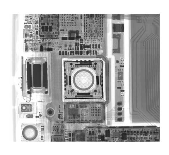
2D X-ray Radiograph of a smartphone camera.
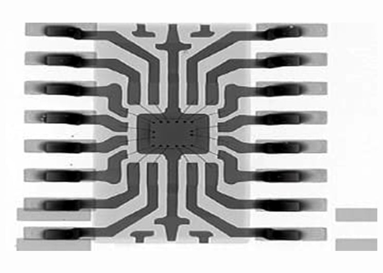
X-ray Radiograph of a still-packaged wire-bonded component. The Lead frame, bond wires, and die are clearly visible.
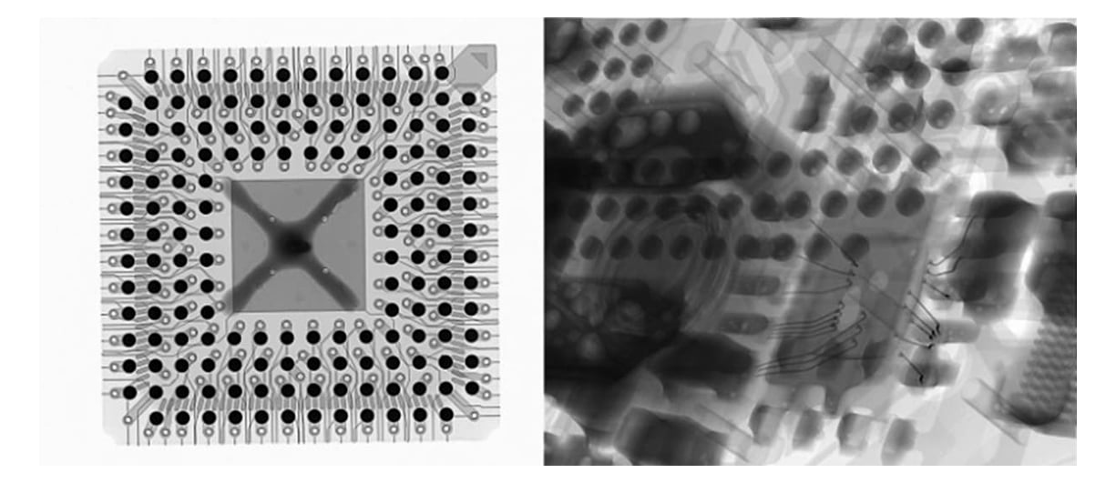
Left: X-ray Radiograph of an unbonded BGA board.
Right: Oblique view of a wire-bonded device and BGA soldered on opposite sides of a PCB. Copper traces, vias, solder balls, and solder voids are clearly visible.
What we accept:
- Requires solid samples or samples that can be glued in place to limit vibrations.
- Samples need to be stable under normal atmospheric conditions.
- Samples need to be a maximum size of 740 x 580 mm (29 x 22.8 inches).
- Samples are limited to a maximum weight of 5 kg (11lbs).
- The inspection area can be up to 510 x 445mm.
Use Cases

Electronics & Semiconductor
Detects solder voids, cracked balls, bridging, lifted wires, and Head in Pillow defects in BGA.
Battery & Energy Storage
Reveals voids, cracks, or delamination in electrodes and seals.

Medical Devices & Biomedical
Ensures proper assembly of miniature implantable devices.

General Materials Science
Identifies inclusions, porosity, and fractures in composites and metals.

PCBA Inspection Services
Identify via misalignment, shorts, and layer defects in complex boards.
Complementary Techniques
- Mechanical Cross-Section: To expose potential defects and understand their origin.
- Micro-CT: Provides a complete 3D reconstruction of the sample for a more detailed internal analysis.
- Optical Microscopy: Ideal for surface-level inspections, where penetrative scanning is unnecessary.
- Scanning Electron Microscopy: Provides high-resolution surface and cross-sectional imaging.
Mechanical Cross-Section Analysis (X-Section)
Uncovers microstructures and defects causing performance issues. Explore
Scanning Electron Microscopy (SEM)
Images surface topography and composition with electrons. Explore
X-ray Computed Tomography (Micro-CT)
Non-contact, non-destructive 2D/3D images at micron scale. Explore
Why Choose Covalent for Your 2D X-Ray Imaging Needs?
Covalent offers industry-leading expertise in 2D X-ray inspection, delivering rapid results for PCB and BGA X-ray inspections. Our team tailors X-ray metrology conditions for each project, ensuring reliable detection of solder voids, interconnect failures, and subtle assembly defects.
Whether you need fast PCBA inspection services or in-depth non-destructive failure analysis, our solutions provide clarity and actionable insight.
Frequently Asked Questions
Identifying the right test can be complex, but it doesn’t have to be complicated.
Here are some questions we are frequently asked.
What is the difference between 2D, 2.5D, and 3D X-ray inspection?
- 2D X-ray (radiography): Produces flat projection images, ideal for fast PCB X-ray inspection but limited by feature overlap.
- 2.5D X-ray inspection: Collects angled projections through oblique-view geometry to create depth-resolved images, reducing feature overlap and improving defect detection in BGA X-ray inspection and multilayer PCBs.
- 3D CT: Reconstructs a full volumetric model, providing the most complete data but with longer scan times.
Can a 2D X-ray detect solder voids and BGA connectivity issues?
Yes. 2D X-ray inspection reveals solder voids, poor wetting, and interconnect failures in BGAs. While CT provides more precise volumetric void measurements, 2D imaging delivers rapid and reliable screening for quality control.
How does 2D X-ray inspection compare in speed and accuracy to 3D CT?
- Speed: 2D X-ray imaging is faster, ideal for PCBA inspection services and high-throughput testing.
- Accuracy: It provides clearer in-plane detail than 2D radiography, but CT is more accurate for a complete volumetric analysis.
What spatial resolution and feature sizes can 2D X-ray resolve?
Modern 2D X-ray inspection systems can resolve features in the low-micron range, making them ideal for analyzing solder joints, cracks, and interconnects in PCB X-ray inspection and BGA X-ray inspection, as well as batteries, metal parts, medical devices, and more.
What sample size or geometry limits apply to 2D X-ray inspection?
Typical systems can handle boards up to ~740 × 580 mm and weights up to 5 kg. Very dense or thick samples may require CT instead of oblique X-ray metrology.
When should I choose 2D or 2.5D X-rays over a 3D Scan?
Choose 2D X-ray inspection when a full 3D CT scan is unnecessary or time-consuming. It is ideal for multilayer PCB X-ray inspection and BGA X-ray inspection, providing depth-resolved images that reveal hidden solder voids, cracks, and Head in Pillow defects without destructive cross-sectioning.