What Is Atomic Force Microscopy (AFM)?
AFM is a high-sensitive and high-resolution scanning technique that maps materials’ surface topography and properties with sub-nanometer vertical accuracy. As part of the broader Scanning Probe Microscopy (SPM) family, atomic force microscopy techniques stand out for their ability to capture chemical, electrical, mechanical, and magnetic characteristics, often in a single scan.
An AFM tip, typically 2-20 nm in radius, protruding from a flexible cantilever interacts with the sample surface responding to Van der Waal’s, magnetic, and electrostatic forces. As the tip interacts with the sample’s surface, it responds to Van der Waals, magnetic, and electrostatic forces. These deflections are captured by an optical system that reflects a laser off the back of the cantilever into a detector, translating molecular-level interactions into quantifiable maps.
At Covalent, we tailor our analysis to the scale, complexity, and failure modes across semiconductor, battery, and biomedical industries.

High Resolution
High Resolution
Atomic z‑resolution (~0.1 nm) and nanometer lateral resolution.

Multimodal
Multimodal
Advanced modes uncover chemical, mechanical, and electrical properties.

Non‑Destructive
Non‑Destructive
Tapping and non-contact modes preserve delicate or soft samples.
Why Use AFM?
AFM excels when nanoscale behavior drives performance and when other techniques fall short. It enables mapping of vertical deviations, surface interactions, and electrical/chemical domains without damaging sensitive samples.

Material Performance
Identifies nanoscale failure points and mechanical/electrical behaviors.

Unique Resolution
Provides vertical accuracy when optical methods cannot.

Industry Relevance
Used in semiconductors, batteries, consumer electronics, biomedical, renewable energy, food, and drug sectors.

Working Principle
AFM atomic force scanning uses an ultra-sharp probe tip, mounted on a cantilever, across the sample in a raster pattern. The surface forces bend or oscillate the cantilever, and a reflected laser captures these movements in real time.
A feedback loop maintains constant force between the tip and the surface, enabling precise 3D mapping of topographical features at angstrom-level sensitivity.
AFM operates across multiple imaging modes, and each offers unique insights:
- Contact Mode: The tip maintains continuous contact with the surface. Best for rigid samples.
- Tapping Mode (Non-Contact): The tip oscillates near its resonance frequency, minimizing surface damage to soft materials.
- Conductive AFM (C-AFM): Measures current flow through the tip to map nanoscale conductivity.
- Magnetic Force Microscopy (MFM): Detects long-range magnetic interactions, revealing magnetic domains.
- Electrostatic Force Microscopy (EFM): Visualizes and maps surface charge distributions via electrostatic forces.
- Kelvin Probe Force Microscopy (KPFM): Analyzes contact potential difference, estimating surface work function.
- Force Spectroscopy & Force-Volume Mapping: Quantifies adhesion, stiffness, and elastic modulus at specific surface sites.
- Piezo Force Microscopy (PFM): Probes piezoelectric and ferroelectric domains in functional materials.
- Quantitative Nanomechanics (QNM): Measures nanoscale stiffness and modulus with enhanced repeatability across heterogeneous surfaces.
These modes turn AFM from a topography tool into a multimodal platform for material property discovery.
Equipment Used for AFM:
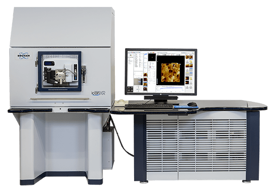
Bruker Nano Dimension (with Icon and FastScan Heads)
- 200 mm stage for wafer and device-level analysis.
- Scan speed: Up to 20 Hz, enabling high-throughput imaging without loss of resolution.
- Vertical noise floor: < 30 pm RMS ensuring sub-nanometer precision.
- AFM modes: Comprehensive suite including ScanAsyst, TappingMode (air/fluid), Phase Imaging, Lateral Force Microscopy, MFM, EFM, Kelvin Probe Force Microscopy, Peak Force Tunneling AFM (TUNA), Force Spectroscopy, and PeakForce Quantitative Nanomechanical Mode (QNM).
- TRC: Spreading Resistance Microscopy, Scanning Capacitance Microscopy.
Key Differentiators
Atomic force microscopes deliver data at a scale where even minor variations in surface can influence functionality or failure.
- Data Outputs: Topography, surface roughness, conductivity, work function, capacitance, modulus, coercivity, adhesion, and charge.
- Sensitivity: Noise floor ~0.05 nm RMS; Vertical range: 0.1 nm to 10 µm.
- Resolution: Lateral (XY): 2–10 nm; Vertical (Z): ~0.1 nm.
- Material Compatibility: Optimized for solids and flat surfaces; some modes operate in liquid environments.
- Depth Profiling: Not standard, but interface mapping is possible via angle-lapping or cross-sectioning.
At Covalent, we extend these outputs into targeted and comparative diagnostics, turning surface data into answers and insights that matter.
Strengths
AFM combines mode versatility, high vertical sensitivity, and nanoscale resolution. Covalent optimizes this capability through strategic execution:
- Application Range: Works across conductive, insulating, soft, fragile, or layered materials.
- Mode Breadth: From force spectroscopy and nanomechanics (QNM) to charge mapping and piezoelectric imaging (PFM), workflows adapt to a wide variety of materials and conditions.
From force spectroscopy to charge mapping, our AFM atomic force workflows are built around the physics of your material and the metrics that define success.
Limitations
AFM is powerful, but context matters:
- Scan Area: Limited to ~90×90 µm.
- Speed: Slower than widefield optical profilometry.
- Sample Geometry: Curved or unstable surfaces pose challenges.
- Tip Lifetime: Artifacts may arise from tip wear or contamination.
- Liquid Imaging: Requires dedicated probes and environments.
We assess feasibility before every scan to ensure the correct method, mode, and output.


Sample Information
A typical AFM dataset provides multiple co-registered images, each reflecting distinct nanoscale material properties. In the example below, three output channels are displayed: topographic height, adhesion, and peak force TUNA current, captured from a microporous carbon electrode used in hydrogen fuel cells.
The electrode consists of carbon black particles bound by a Teflon-like polymer. While this binder improves mechanical integrity and membrane adhesion, it can reduce through-plane conductivity and lower fuel cell performance.
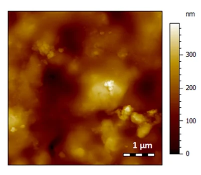
Topographic Height
Atomic resolution HAADF and Optimized bright field (OBF)-STEM images of electron beam irradiation sensitive materials, which cannot be acquired by conventional STEM.
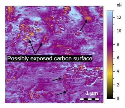
Adhesion Map
Adhesion is measured during tip retraction. Areas of low adhesion may indicate exposed carbon, while high-adhesion zones are likely binder-rich. This map highlights variations in local chemistry and surface energy across the film.
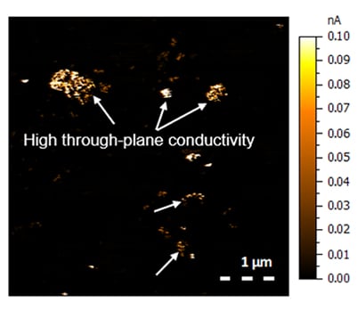
Peak Force TUNA Current
The current image reveals conductive pathways within the electrode. Regions with measurable current indicate locations where electrical flow is supported, which is vital for assessing functional continuity in electrochemical materials.
Together, these images provide a multidimensional view of surface structure, mechanical behavior, and electrical performance, enabling rapid imaging, defect localization, and in-depth material diagnostics at the nanoscale.
What we accept:
Accurate AFM starts with precise preparation. We guide clients through every step to minimize errors and optimize signal quality.
- Form: Solids are preferred, but liquids are compatible for certain biological applications.
- Stability: Air or Liquid compatible (Example: Water, PBS).
- Size: The ideal sample size is ~1×1 mm. Larger wafers can be mounted directly.
- Prep: May require cleaving, gluing, or fiducial markers for targeting.
Need help preparing your sample? Our team designs mounting protocols based on material type, fixture, and imaging goal.
Use Cases
Semiconductor
Sidewall profiling, dopant mapping, gate oxide failure analysis.

Energy Storage
Electrode roughness, degradation tracking, conductive area mapping.
Polymers & Coatings
Phase distribution, film uniformity, stiffness gradients.

Biomedicine
Cell-substrate adhesion, hydrated modulus, nanoscale morphology.
Complementary Techniques
In a broader surface characterization workflow, AFM is often the primary resolution. For deeper insights, it is commonly paired with:
- AFM-IR (Photo-induced Force Microscopy): Combines AFM’s spatial resolution with IR spectroscopy’s chemical sensitivity, making it effective for analyzing delicate organics or heterogeneous materials.
- FTIR (Fourier Transform Infrared Spectroscopy): Useful for identifying organic compounds and analyzing thin film coatings.
- Optical Profilometry by Laser Confocal or White Light Interferometry: For surface topography and surface roughness with a larger field of view. It can be useful if the surface is both wavy and rough, which is common in alloys, polymer composites, and non-uniform film deposition.
- Raman Spectroscopy: Offers complementary vibrational information, particularly valuable for characterizing crystalline or polymeric structures.
- SEM-EDS (Scanning Electron Microscopy with Energy-Dispersive X-ray Spectroscopy): For top-down surface imaging and elemental composition mapping, especially for conductive or metallized samples. Other spectroscopic tools like Auger emission analysis can also be used for ultra-surface-sensitive elemental characterization where nanometer-scale resolution is required.
- Spectroscopic Ellipsometry (SE): Measures film thickness and optical properties over larger areas, complementary to AFM’s localized resolution.
- XPS (X-ray Photoelectron Spectroscopy): Provides surface-sensitive chemical and oxidation state analysis, ideal for layered or functionalized surfaces.
- X‑ray Reflectivity (XRR): Provides nanometer‑scale film thickness and density measurements, ideal for correlating with AFM roughness data.
These complementary techniques are chosen based on the resolution needed, material, and failure mode. If you have difficulties choosing the right one, we can always advise on the best combination for the best results.
Photo-induced Force Microscopy (PiFM)
Nanoscale chemical characterization & topography at sub-5nm. Explore
Raman Spectroscopy
Measures inelastic photon scattering for chemical identification. Explore
Spectroscopic Ellipsometry (SE)
Measures thin-film thickness & optical properties. Explore
White Light Interferometry (WLI)
Measures surface topography with sub-nanometer vertical resolution. Explore
X-ray Photoelectron Spectroscopy (XPS)
Measures surface elemental composition and chemical states. Explore
X-ray Reflectometry (XRR)
Optimized scans tailored to each sample for best measurements. Explore
Why Choose Covalent for Your AFM Needs?
Covalent’s atomic force microscopy services deliver more than just surface maps; they yield interpretation, correlation, and actionability. Here’s what sets us apart:
- Multimodal Expertise: We operate across advanced AFM modes. From KPFM and MFM to force-volume mapping, tailoring each scan to the physics of your sample.
- High Sensitivity & Resolution: Our Bruker Dimension Icon with FastScan delivers rapid, sub-nanometer mapping across large formats and fine features.
- Consultative Approach: Our scientists collaborate with you on every scan, from sample prep to mode selection to results interpretation.
- Integrated Workflows: We design AFM analysis as part of an integrated suite, correlating findings with SEM-EDS, FTIR, or XPS as needed.
- Reliable Tip Protocols: Each project begins with a fresh tip, and we monitor artifacts in real time to maintain integrity.
- Reference Standards Available: For advanced imaging or calibration, we offer step-height standards and custom references.
- Flexible Mounting & Prep: We support challenging geometries and fragile samples with custom-built fixtures and prep strategies.
Whether you need nanoscale insight into a failure, a process, or a material interaction, our AFM systems and team of experts deliver data engineered for decisions.
Frequently Asked Questions
Identifying the right test can be complex, but it doesn’t have to be complicated.
Here are some questions we are frequently asked.
What scan size is preferred?
Scan size depends on the material and surface uniformity. For atomically smooth surfaces like silicon, a 2 × 2 µm scan size at 512 × 512 pixel resolution is standard.
What pixel resolution do you use?
We typically use 512 × 512 pixels, balancing resolution and speed. However, larger scan sizes require extended time and increased total cost. For more detailed information, we recommend emailing us.
Do you use a fresh tip for every scan?
Yes. Every project begins with a fresh AFM tip. If any artifacts are observed during the project, these tips will also be replaced.
Can you provide a calibration reference?
Yes. We typically use step-height reference standards for calibration and have different reference standards for advanced imaging modes. For more detailed information, we recommend emailing us.

Resources