What Is Surface and Interface Testing?
The surface of a material is where the action is. It is where the performance begins, and often where it fails. This is where bonds are either formed or broken, adhesion takes hold, and corrosion begins. Interfaces, however, operate behind the scenes: the internal boundaries where two materials meet, exchange energy, or fall apart.
Surface and interface testing focuses on these critical parts of a material: the outermost nanometers and the junctions between the layers. Using a suite of precision techniques, such as X-ray Photoelectron Spectroscopy (XPS), Atomic Force Microscopy (AFM), Time-of-Flight Secondary Ion Mass Spectrometry (ToF-SIMS), ellipsometry, nanoindentation, and others, these tests measure roughness, film thickness, surface chemistry, adhesion, energy, and more.
These tests reveal quantitative data that support failure analysis, process validation, and material qualification. At Covalent, surface and interface analysis is integrated across other techniques to link surface phenomena to overall system performance.
Why Invest in Surface and Interface Testing?
Surface and interface testing offers engineers direct insight into what’s working, what isn’t, and why by capturing the origin point of material behavior.
Core benefits include:
- Validating Product Performance: Confirming bond strength, coating durability, and interfacial reliability under real-world operating conditions.
- Preventing Costly Failures: Detecting early-stage issues like contamination, surface defects, or poor adhesion that often trigger delamination, corrosion, or warranty events.
- Optimizing Material and Supplier Selection: Using quantitative surface metrics to guide vendor approval and refine manufacturing parameters.
- Accelerating R&D and Innovation: Fine-tuning new materials, multi-layer designs, and advanced coatings to meet performance targets in next-gen systems.
Integrating surface and interface testing early in development reduces risk, streamlines validation, and advances product readiness.
When Should Surface and Interface Testing Be Performed?
Surfaces evolve and respond to their environments, fabrication steps, and treatments. The testing schedules must be tightly aligned with these transitions to yield accurate and actionable data.
Covalent recommends surface and interface testing during:
- Initial Process Development: Establishing a measurable surface baseline.
- Post-deposition or Cleaning Steps: Assessing treatment outcomes.
- Supplier Evaluation: Verifying batch consistency across lots.
- Pre- and Post-treatment Validation: Confirming chemical or mechanical surface changes.
- Environmental Exposure Studies: Assessing the impact of humidity, solvents, or thermal cycling.
- Failure Analysis: Identifying breakdowns at adhesion or material junctions.
- Regulatory Submissions and Incoming Inspection: Supporting compliance and quality verification.
We tailor our surface and interface analysis to each test, guided by sample type and objective, to achieve fast, reliable, and maximally insightful results.
Industries That Use Surface and Interface Testing
Surface integrity and interface performance are fundamental in sectors where material function is critical:
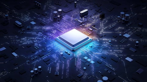
Semiconductors
Interface mapping, oxide thickness control, and residue detection.
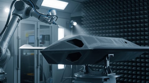
Aerospace
Surface prep validation, thermal barrier evaluation, and corrosion onset studies.

Medical Devices
Passivation layer characterization and biocompatibility verification.
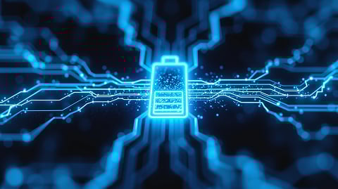
Energy Storage
Electrode coating conformity, aging behavior, and layer integrity.
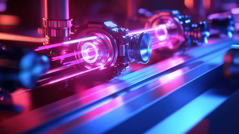
Optics & Photonics
Thin-film stack assessment, refractive accuracy, and bonding uniformity.
Key Differentiators
Advantages
- Compatible with a wide range of materials, including polymers, metals, ceramics, and composites
- Sensitive to nanoscale surface and interface variations
- Enables non-destructive or low-impact testing for delicate samples
- Quantifies key surface metrics such as roughness, chemistry, and energy
- Supports continuous process improvement and material innovation workflows
- Enables real-time or in-line testing to improve process control
Surface and interface testing offers clarity. Not conjecture, not inference, but quantitative, high-resolution insights that tie microstructural phenomena to real-world outcomes.
Limitations
Like any other analytical approach, surface and interface testing has boundaries defined by physics, instrumentation, and context. Selecting the correct method and preparing the sample correctly are critical to obtaining meaningful results. Some key limitations include:
- Most methods require flat, vacuum-compatible, or conductive surfaces
- Polymers and organics may degrade under electron or ion beams
- Surface-level data may not reflect the properties of bulk material
- Results often require validation through complementary techniques
- Sample preparation and handling must follow strict protocols to avoid contamination or artifacts
- Depth-profiling methods (for example, sputtering) can be destructive
- Some instruments require specialized training or lab environments for proper use and maintenance
Consult with our scientists at Covalent to ensure the method aligns with the material, failure mode, and question at hand.
What Properties Are Measured in Surface and Interface Testing?
Surface and interface testing measures the physical and chemical characteristics that govern performance, durability, and reliability at material boundaries.
Typical outputs include:
- Interfacial adhesion strength between bonded layers or dissimilar materials.
- Surface contamination: Particulate matter, organic films, or inorganic residues.
- Chemical composition, oxidation states, and bonding environments.
- Surface roughness and nanoscale topography.
- Morphological uniformity; defect detection, such as pinholes, voids, or delamination.
- Film thickness and conformity across coatings and multilayer stacks.
- Degree of crystallinity or amorphous structure near the surface.
- Surface-level electrical properties like work function and potential.
- Mechanical properties: Surface hardness, modulus, and response to localized force.
Whether you need to qualify coatings, engineer a more reliable multi-material system, or optimize treatments, surface and interface testing gives you that data.
How Are Results Tracked and Reported?
Data alone doesn’t solve engineering problems. Interpretation does. At Covalent, we combine raw measurements with interpretations, from spectra and morphology to root-cause insights. Our clients receive method details, annotated data, precise conclusions, and access to raw files and on-demand one-on-one sessions with our experts.
Our reports include:
- High-resolution spectra, maps, and profile outputs.
- Layer-specific analysis of composition, thickness, or topography.
- Quantified measurements with precision calibration.
- Interpretation aligned to process stages or failure modes.
- Structured outputs, suitable for QA, regulatory, and development workflows.
Types of Surface and Interface Testing
| Measurement Type | Property Assessed | Applications |
|---|---|---|
| Topography & Roughness | Surface texture and morphology | Adhesion prep, wear resistance, bonding surfaces |
| Surface Energy | Contact angle, hydrophobicity | Coating quality, adhesion optimization |
| Chemical Composition | Elemental and molecular identity | Contamination, oxidation, cleaning effectiveness |
| Film Thickness & Index | Layer depth, refractive index | Conformal coatings, multilayer analysis |
| Layer Transitions & Interfaces | Structural variation between layers | Diffusion, delamination, structural defects |
| Mechanical Properties | Hardness, modulus | Scratch resistance, mechanical wear |
| Crystallinity & Phase | Grain orientation, phase structure | Thin film integrity, stress behavior |
| Electrical Properties | Conductivity, surface potential | ESD analysis, device reliability |
| Adhesion Strength (optional) | Interlayer bond strength | Peel/pull-off tests, coating validation |
Typical Applications
Surface and interface testing supports various validation, troubleshooting, and optimization needs. Common use cases include:
- Verifying plasma treatment or chemical cleaning effectiveness.
- Assessing adhesion layer thickness and conformity.
- Identifying surface residues and unknown contaminants.
- Analyzing multilayer stack composition and oxide thickness.
- Detecting corrosion initiation, delamination, or interface fatigue.
Why Choose Covalent for Surface and Interface Testing Services?
Covalent’s surface and interface testing lab is equipped with a comprehensive suite of tools, such as XPS, AFM, ellipsometry, nanoindentation, and more, built to analyze diverse materials with precision and speed. Our scientists bring expertise in surface characterization, interface mechanics, and thin film analysis to every project. Each test is custom-designed to match the material, objective, and scale of analysis. From method development to data interpretation, we focus on delivering high-resolution results that are fast, clear, and engineered for action. Ready to get started? Request a quote or talk to our team.
Frequently Asked Questions
Can I send multiple sample types in one batch?
Yes. We routinely analyze different materials within a single project, using method-matched workflows tailored to each sample’s structure and testing objective.
What's the typical turnaround time?
Most surface and interface testing projects are completed within 5–10 business days, depending on complexity, volume, and sample preparation requirements.
Is testing destructive?
How do I prepare samples for surface testing?
Avoid contamination by handling samples with clean tools and gloves. Some methods also require flat, dry, vacuum-compatible surfaces, but there is no need to stress. Our team will walk you through exactly what’s needed as part of the intake process.
Related Techniques for Surface and Interface Testing
No technique can tell the full surface story. At Covalent, we apply a suite of complementary tools with surface and interface testing, each based on the material type, resolution needed, and the objective.
- AFM (Atomic Force Microscopy): Provides nanoscale surface topography, roughness measurement, and phase contrast imaging.
- Ellipsometry: Measures thin film thickness, refractive index, and other optical constants with high precision.
- Nanoindentation: Evaluates mechanical properties such as hardness and elastic modulus at micro- and nano-scales.
- ToF-SIMS (Time-of-Flight Secondary Ion Mass Spectrometry): Analyzes surface contamination, trace elements, and isotopic or molecular mapping at extremely high sensitivity.
- XPS (X-ray Photoelectron Spectroscopy): Used to determine elemental composition, chemical states, and oxidation levels on material surfaces.
Together, these methods resolve geometry, chemistry, and function from the nano- to microscale.
Atomic Force Microscopy (AFM)
Maps nanoscale topography and material properties with a sharp probe. Explore
Time of Flight Secondary Ion Mass Spectroscopy (ToF-SIMS)
Ultra-sensitive surface analysis with chemical imaging & depth profiling. Explore
X-ray Photoelectron Spectroscopy (XPS)
Measures surface elemental composition and chemical states. Explore


Resources