Apr 02 2021, 6:00 am
ABSTRACT In this application note, Dr. Frazer summarizes the impact of offcut angle on thin film growth, and goes on to detail the process by which offcut angle is analyzed using X-ray Diffraction (XRD). Each step of this industry-standard procedure is demonstrated on a NIST standard Al2O3Â sample wafer, and the computation of the offcut angle is provided for ready reference.
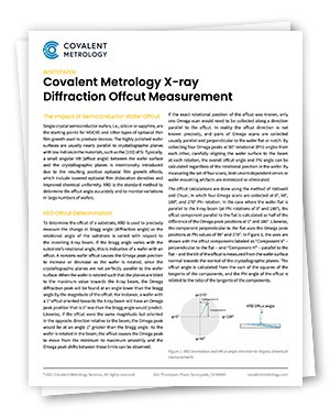
The wafer offcut angle (the small angular tilt between the wafer surface and its internal crystallographic planes) affects key growth properties of epitaxial thin films grown on these substrates for use in modern semiconductors and advanced electronic devices. Efficient, precise measurement of the substrate offcut angle can empower engineers to refine their processing and fabrication techniques and optimize performance in their end products.
Covalent’s Director of X-ray Analysis, Dr. Colleen Frazer, assembled this Application Note to equip you with the expertise needed to navigate offcut angle measurements like a pro.
Learn more about X-ray Diffraction (XRD)
Read the Blog: Recommended Strategies for Wafer Offcut Measurement in Thin Film Applications Using X-ray Diffraction (XRD)