What Is Atomic Resolution Electron Microscopy (AEM)?
Atomic Resolution Analytical Electron Microscopy (AEM) is an advanced form of electron microscopy that combines the ability to directly visualize individual atoms within a material with simultaneous analytical capabilities for determining elemental composition and chemical state at the atomic scale. Our atomic resolution STEM features multiple state-of-the-art, highly sensitive detectors that leverage various interactions between the incident electron beam and the sample, enabling comprehensive investigation of physical properties such as dimensions, crystal structure, elemental composition, bonding structure, and stress, even in materials that are fragile under electron beam irradiation, while achieving sub-nanometer spatial resolution.

Atomic‑Scale Imaging
Atomic‑Scale Imaging
Resolves individual atoms, defects, and interfaces with aberration‑corrected STEM for sub‑nanometer metrology.

Correlated
Chemistry
Correlated Chemistry
Maps elemental composition and bonding/electronic states via simultaneous EDX/EELS, aligned to the same atomic‑scale features.

Nano‑Scale
Strain Mapping
Nano‑Scale
Strain Mapping
Quantifies local stress/strain with precession electron diffraction (PED), revealing device‑relevant lattice distortions.
Why Use AEM?
- High spatial resolution, detection sensitivity, and data reliability. When the spatial resolution achievable with conventional STEM is insufficient, atomic-resolution AEM provides the necessary performance.
- Accurate stress mapping with nanometer-scale resolution. Precession Electron Diffraction (PED) enables precise evaluation of stress distributions at the nanometer level.
- Improved analysis of beam-sensitive materials. Our atomic-resolution AEM is beneficial for specimens that are easily damaged by electron-beam irradiation during conventional STEM, EDX, or EELS analysis.
- High-precision metrology, elemental composition, and bonding/electronic structure characterization. AEM enables detailed structural, compositional, and electronic analysis with sub-nanometer resolution.

Sub-Nanometer Metrology
Measures critical dimensions and interface abruptness at atom‑level precision for next‑gen devices and nanomaterials.

Aligned Chemistry and Structure
Correlates atomic‑resolution images with EDX/EELS maps to link composition, bonding, and defects to performance.

Sensitive to Beam-Fragile Samples
Optimized detectors and conditions capture atomic data from irradiation‑sensitive materials with minimal damage.

Working Principle
Atomic Resolution Analytical Electron Microscopy utilizes a scanning transmission electron microscopy (STEM) equipped with a spherical aberration corrector, allowing for direct observation and analysis of specimens at atomic resolution, including nano-meter order stress analysis through precession electron diffraction. The system integrates advanced analytical techniques such as STEM, Energy Dispersive X-ray Spectroscopy (EDX), electron energy-loss spectroscopy (EELS), and precession electron diffraction (PED).
Unlike conventional STEM imaging, atomic resolution and stress analyses require optimization of measurement conditions and lamella specimen thickness, which are only possible with sophisticated techniques.
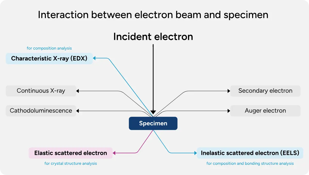
- Analytical Depth: Spatially resolved EDX and EELS spectra having information about elemental composition and bonding/electronic structure (band gap) with STEM images. 2-dimensional map or line profile can also be provided. 2-dimensional strain map by PED patterns analysis.
- Material Compatibility: Solid specimens must be thinned to a thickness of less than 100 nm.
- Spatial Resolution: 53 pm (= 0.053 nm) in STEM, EDX and EELS. 2 nm in stress analysis using PED.
- Depth Profiling: Any depth region can be accessed using cross-sectional sample.
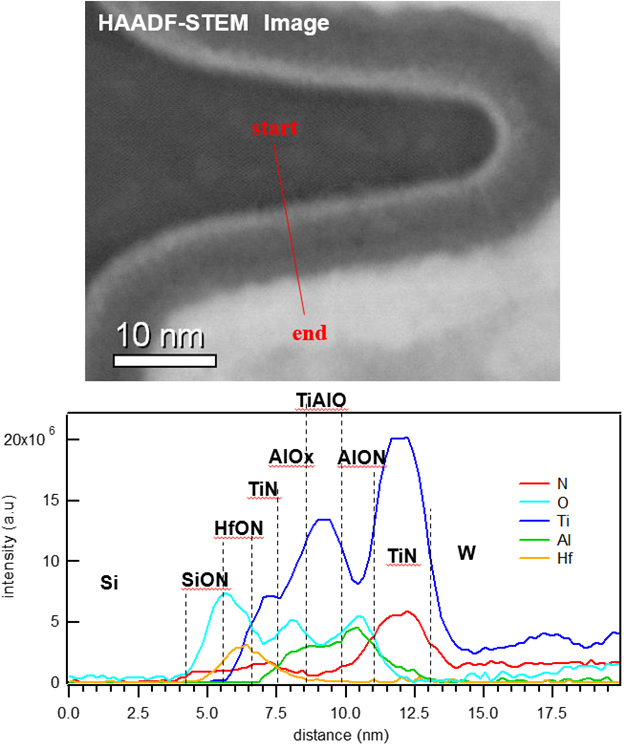
Elemental distribution along the red line in finfet structure using EELS.
In elemental composition analysis, the detection limit can be improved to 0.1 atom% using highly efficient detectors and reducing noise in spectra. The detection limit of strain analysis is 0.1% in terms of lattice spacing difference.
Equipment Used for AEM:
JEOL ARM300F2
- Accelerating voltage: 40-300 kV.
- Delta-type spherical aberration corrector for STEM.
- Segmented annular all field detector for OBF (optimum bright field)-STEM imaging.
- Dual SDD-type EDX detectors with large window, 158 mm2.
- Gatan Continuum S for high-speed EELS detection.
- EDM (Electrostatic Dose Modulator) fast beam blanking system.

JEOL ARM200F
- Accelerating voltage: 80-200 kV.
- NanoMegas ASTAR for ACOM-TEM.
- Gatan GIF Quantum ER for EELS detection.
- STEM-HAADF resolution: 78 pm at 200 kV with cold FEG (82 pm with Schottky).
- Built-in STEM probe Cs-corrector enabling high probe current for atomic‑resolution EDS/mapping.
- Elemental analysis served with JEOL’s own wide area (100 mm2) Silicon Drift Detector (SDD) provides high-speed and high-sensitivity of detection.

Key Differentiators
Atomic-scale imaging resolution enables simultaneous structural and chemical analysis, allowing visualization of defects and interfaces at the atomic level. These capabilities are supported by advanced aberration correction and offer wide applicability across disciplines.
Strengths
- When developing semiconductor devices or nanomaterials, any physical properties and dimensions must be evaluated with sub-nm order spatial resolution.
- Carefully acquired EEL spectra give us information about electronic structure such as bandgap and band structure, directly connecting to the semiconductor device/material properties.
- It is possible to consider material or device properties directly from the experimental result regarding local structure, composition and stress.
- It is also possible to provide and share deep considerations regarding material/device properties based on abundant experiences and knowledge.
Limitations
- It is impossible to apply to a gas or liquid sample. It is also difficult to apply fragile materials in the preparation of thin lamella.
- Soft materials are easy to introduce ion-beam milling damage for the thin lamella preparation. So, cryogenic processing or other methods are sometimes employed to preserve their intrinsic structural and chemical properties.
- As for detection sensitivity, SIMS for elemental composition, IR for bonding structure, Raman for stress are better but in any case, AEM has better spatial resolution.


Unsure Whether AEM Is Right for You?
We are a leading advanced materials science and analytical services laboratory offering access to cutting-edge microscopy and characterization tools combined with expert scientific support.
Sample Information
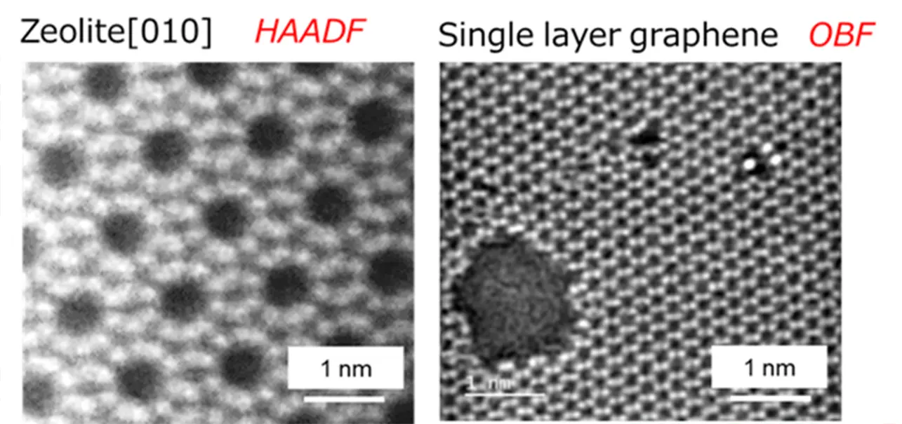
Atomic resolution HAADF and Optimized bright field (OBF)-STEM images of electron beam irradiation sensitive materials, which cannot be acquired by conventional STEM.
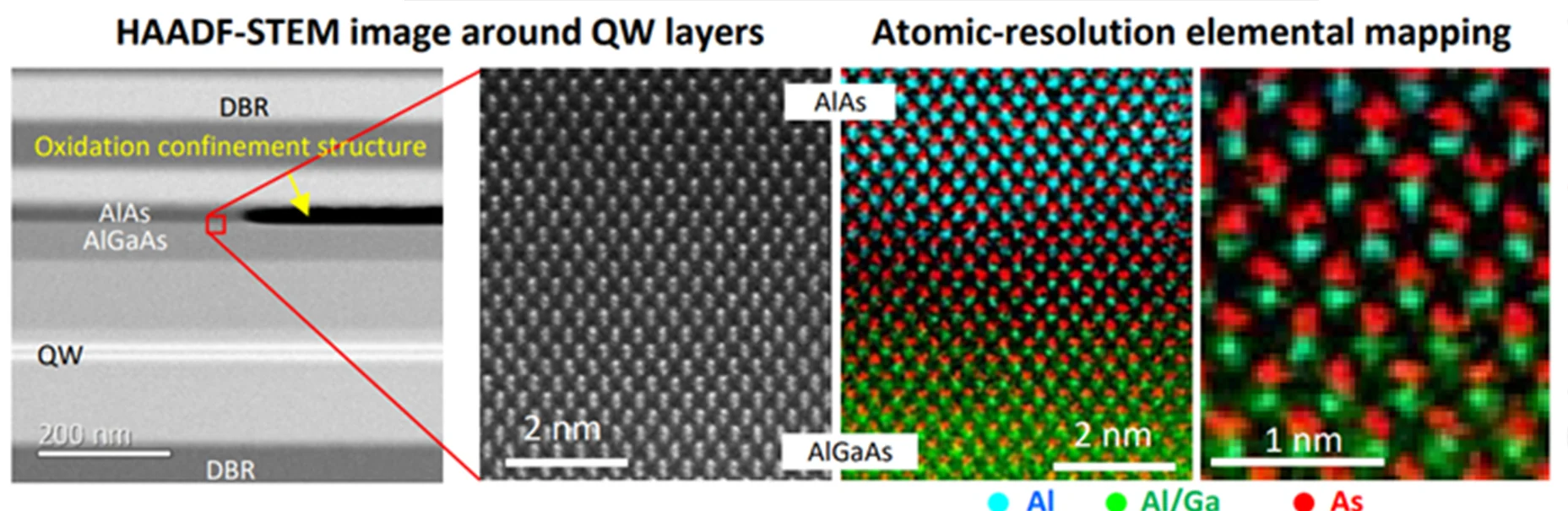
Atomic resolution EDX mapping at AlAs/AlGaAs interface. Elemental diffusion at hetero interfaces can be evaluated with atomic resolution.
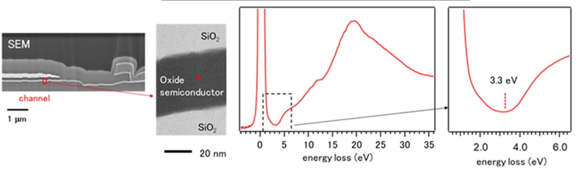
Low-loss EELS spectrum at the semiconductor layer in a thin film transistor (TFT) device, which shows the band gap of the oxide semiconductor. The bandgap energy value and mid-gap state can be compared between several samples.
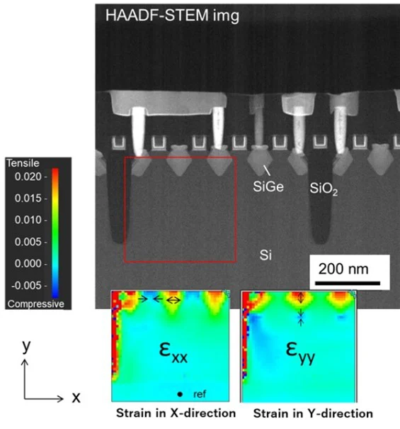
Lattice strain mapping at Si/SiGe using PED technique. The degree of local stress and spatial distribution of stress can be evaluated in a real device structure.
What we accept:
- The sample must be solid.
- Materials whose original properties cannot be altered even in vacuum.
- When the original sample is large, it must be miniaturized and thinned to a lamella to enable AEM measurements.
- Thin lamella preparation must be necessary before AEM measurements.
Use Cases

Semiconductor
Metrology with Sub-nm Accuracy
- Measurement of channel, electrode length, and oxide thickness, including high-k and metal electrodes in FinFET or other latest logic devices.
- Measurement of multilayer thickness in power or optoelectronic devices using III–V semiconductors.
Elemental Distribution Analysis (STEM-EDX and EELS)
- Multi-stack structure identification around high-k and metal gate in logic devices.
- Evaluation of process effects (etching, heating, etc.) through detection of elemental diffusion.
EELS Bonding / Electronic Structure Analysis
- Investigation of metallic or insulating properties.
- Bandgap and mid-gap state evaluation in localized areas.
Stress Analysis
- Confirmation of stress distribution caused by device structures in III–V semiconductor optoelectronic devices, with nanometer-order resolution.

Material Science
Atomic Arrangement Observation
- Crystal structure analysisfor materials such as zeolite, LiLaZrO, and LiCoO₂, including atomic coordinate identification of oxygen atomsin a local area.
Elemental Distribution Analysis (STEM-EDX and EELS)
- Evaluation of core-shell structuresfor a single nanoparticle.
EELS Bonding / Electronic Structure Analysis
- Oxidation state evaluationof a single catalyst particle.
- Refractive index calculation(optical property investigation) of a local area.
Complementary Techniques
- FTIR: Measures molecular vibrational absorptions to identify chemical bonds, functional groups, and crystallinity in bulk or thin films.
- Raman: Detects inelastic photon scattering to reveal molecular vibrations, stress/strain, phase, and crystal quality with micron‑scale resolution.
- SIMS: Sputters surface and measures ejected secondary ions for ultra‑sensitive elemental/isotopic depth profiles at nanometer scales.
- UV‑Vis absorption: Quantifies electronic transitions and band gaps by measuring wavelength‑dependent light absorption in liquids, solids, or films.
- XPS: Uses X‑rays to probe elemental composition and chemical states within ~1–10 nm of the surface.
These techniques have higher detection sensitivity, but AEM has much better spatial resolution.
Fourier Transform Infrared Spectroscopy (FTIR)
Rapid, non-destructive molecular fingerprinting across materials. Explore
Raman Spectroscopy
Measures inelastic photon scattering for chemical identification. Explore
X-ray Photoelectron Spectroscopy (XPS)
Measures surface elemental composition and chemical states. Explore
Why Choose Covalent for Your AEM Needs?
Frequently Asked Questions
Identifying the right test can be complex, but it doesn’t have to be complicated.
Here are some questions we are frequently asked.
What microscopy techniques are integrated in atomic resolution AEM?
Transmission electron microscopy (TEM), Scanning Transmission Electron Microscopy (STEM), and spectroscopic methods such as energy-dispersive X-ray spectroscopy (EDS) and electron energy-loss spectroscopy (EELS).
What are typical applications of AEM?
Studying crystal structures, interfaces, defects, nanoparticles, catalysts, and materials for semiconductors, energy storage, and nanotechnology.
How is atomic resolution achieved?
By sample preparation, using aberration-corrected electron optics, high-stability microscopes, and precise alignment of the electron beam and detectors.
What information can be obtained using atomic resolution analytical electron microscopy?
Atomic structure, elemental composition, chemical bonding, electronic states, and stress and defect distributions at the atomic scale.

Resources