What Is Precession Electron Diffraction (PED)?
Precession Electron Diffraction (PED) is an advanced TEM diffraction technique that improves the quality and reliability of electron diffraction data for crystallographic analysis. In PED, the incident electron beam is slightly tilted and then rapidly rotated (precessed) around the microscope’s optic axis during acquisition, so the recorded diffraction pattern represents an integration over many closely spaced diffraction conditions rather than a single static orientation.

Atomic-Scale Resolution
Advanced crystallography
PED produces diffraction patterns that are closer to the kinematical ideal, making grain analysis more robust.

Multi-Mode Imaging
Complex Phase ID
PED improves pattern interpretability for multiphase, nanocrystalline, and highly textured samples.

Comprehensive Material Analysis
Nanoscale strain mapping
By quantifying tiny shifts in diffraction-spot positions, local lattice distortions (strain) can be computed.
Why Use Precession Electron Diffraction (PED)?
- Averages diffraction over many conditions → reduces dynamical (multiple) scattering
- Produces more nearly kinematical intensities that better reflect crystal structure
- Well suited for phase ID, orientation mapping, texture/strain analysis, and structure determination (especially in nanocrystalline/multiphase materials)
- Supports nanoscale strain mapping via lattice parameter shifts and local distortions
- Improves electron pair distribution function (ePDF) for amorphous materials by boosting the reliability of diffuse scattering for short-/medium-range order analysis

More reliable diffraction data
Beam precession reduces dynamical (multiple-scattering) effects, giving patterns closer to kinematical intensities.

Better phase + orientation mapping
Higher indexing success in complex, nanocrystalline, and multiphase regions.

Quantitative nanoscale insights
Enables local strain/lattice distortion measurements and supports ePDF for short-range order in amorphous materials.

Working Principle (PED)
Precession Electron Diffraction (PED) is performed in a TEM or STEM by slightly tilting the incident electron beam and then rotating it (precessing) in a cone around the microscope’s optic axis while a diffraction pattern is recorded. PED patterns can be collected at each pixel to generate 2D maps of phase, orientation, and local lattice metrics.

Unlike conventional selected-area or nano-beam diffraction—where intensities can be strongly affected by dynamical (multiple-scattering) effects—PED’s angular integration reduces sensitivity to exact crystal alignment and thickness and yields diffraction intensities that are more nearly kinematical, improving the accuracy and reliability of crystallographic interpretation.
Equipment Used for PED:
JEOL JEM-F200 Multi-purpose Electron Microscope
- The JEOL JEM-F200 is equipped with two large-area SDD detectors that simultaneously provide high-sensitivity analysis, with efficient data collection.
- JEOL JEM-F200 with cold-FEG will have high energy resolution (<0.33 eV) with EELS.
- Cold-Field-Emission Gun (CFEG) Electron Source.
- Accelerating Voltage: 80 kV or 200 kV.
- High current and beam stability = ultra-high spatial resolution.
- TEM Point Resolution: 0.19 nm.
- STEM-HAADF Resolution: 0.14 nm.
- High-res Electron Energy Loss Spectroscopy (EELS).
- Fine Structure/Oxidation State Determination.
- Plasmon Resonance Analysis (CFEG supports zero-loss peak).
- Gatan GIF Continuum ER Image Filter for Energy Filtered TEM (EFTEM).

Key Differentiators
While both PED and 4D STEM deliver crystallographic insights, each has its own strengths and trade-offs. Understanding their differences helps in choosing the right technique for specific materials and analytical goals.
| PED | 4D STEM |
|---|---|
| What it is: Diffraction method where the probe is tilted and rotated (precessed) to average diffraction conditions and make patterns easier to interpret. | What it is: STEM scan where you record a full diffraction pattern at every probe position (2D real-space scan × 2D diffraction = “4D” dataset). |
| Best for: Robust phase/orientation mapping and crystallography workflows; can support strain mapping from spot shifts with good indexing stability. | Best for: A dense diffraction “data cube” (pattern at each pixel) enabling many reconstructions after the fact (virtual imaging, CoM, ptychography, etc.). |
| Main output: A diffraction pattern (or pattern-per-pixel if scanned), typically cleaner and more indexable due to precession averaging. | Main output: Images (BF/ADF/HAADF) and spectra/maps (EDS/EELS). |
| Key tradeoff: Precession simplifies diffraction but can blur fine dynamical details. | Key tradeoff: More data + compute + dose management; results depend heavily on detector performance and analysis choices—powerful but less “push-button.” |
Note: The Nanomegas ASTAR system can be used for 4D-STEM studies.
Strengths
- Reduces dynamical (multiple) scattering, giving diffraction intensities that are more XRD-like and easier to interpret.
- Enables ab-initio structure solution for unknown/small nanocrystals.
- Improves phase/orientation mapping (SPED) with higher indexing rates and better map quality than conventional TEM diffraction.
- More tolerant of specimen thickness/bending than CBED; supports nm-scale strain/phase/orientation analysis.
Limitations
- Requires specialized PED hardware (precession unit/scan coils) and often fast detectors.
- Destructive, elaborate sample prep for bulk specimens (typically FIB lamella).
- Limited sampling area/volume (thin lamella, small ROI) → may need multiple sites for statistics.
- Precession angle has tradeoffs: larger angles improve “kinematical” behavior but can cause Laue-zone overlap.


Unsure Whether TEM Is Right for You?
Learn more about using Transmission Electron Microscopy services today.
Sample Information
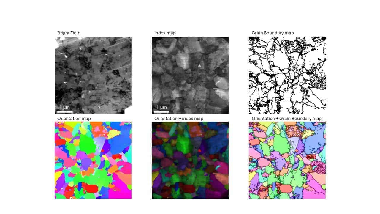
PED used for phase identification of nanocrystalline material.
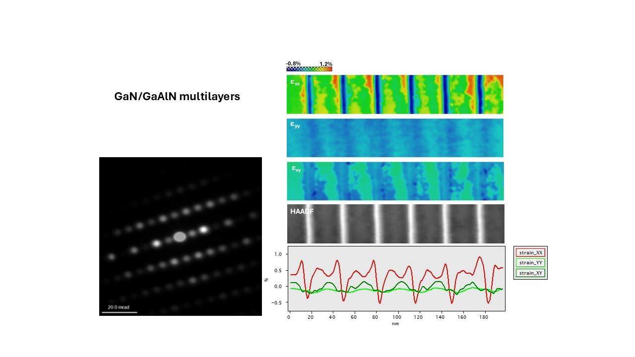
PED for nanoscale strain mapping
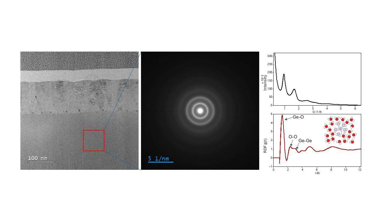
PED can be used to characterize Pair Distribution Functions (pdf) for studying local order on amorphous materials.
What we accept:
-
Thin transparent lamella with a thickness below 100 nm.
-
Bulk sample that is conductive or can be coated with a conductive material for lamella preparation with a focused ion beam.
-
PED can also be done on powders and other nanoscale sample types.
Use Cases

Semiconductor
- Strain and lattice-rotation mapping in advanced devices: quantify local strain in Si/SiGe, FinFET/GAA features, stressors, epi layers.
- Phase + orientation mapping in thin films: texture/grain mapping of TiN, W, Cu, Co, Ru, HfO₂/HZO, etc., tied to resistivity and reliability.
- Defect/crystal quality mapping in epitaxy: correlate dislocations, mosaicity, and local misorientation in GaN/SiC and complex heterostructures.

Consumer Electronics
- Phase/orientation mapping in micro-solders and interconnects: Sn-based solders, intermetallic growth, texture effects tied to drop/shock and thermal cycling.
- Texture/grain mapping in thin-film coatings: hard coatings, decorative/functional layers, and corrosion barriers where grain structure drives durability.
- Crystallization + local order studies in glasses/amorphous layers: ePDF-enabled local-order characterization for amorphous oxides or glassy coatings used in displays/sensors.

Aerospace & Defense
- Microstructure-to-performance in high-temp alloys: map phases/orientations in superalloys and refractory alloys to understand creep/oxidation behavior.
- Ceramics and armor materials characterization: identify phases/orientations in SiC, Al₂O₃, B₄C, ZrO₂ to link processing to toughness.
- Radiation/thermal damage studies: quantify local lattice distortion and defect-related misorientation after extreme environments.

Battery research
- Phase mapping during cycling: track phase transformations in cathodes/anodes (layered ↔ spinel/rocksalt, etc.) at the nanoscale.
- Local strain and lattice distortion near interfaces: measure deformation at particle boundaries, coatings, and reconstructed surface layers that drive fade.
- Characterizing nanoscale heterogeneity in multiphase particles: resolve orientation/phase domains inside single particles to connect microstructure to kinetics.

Failure analysis
- Phase identification of “mystery” features: identify unexpected crystalline phases in residues, corrosion products, precipitates, or reaction layers.
- Interfacial reaction layer mapping: map phase/orientation changes across interfaces (metal/oxide, solder/UBM, barrier/liner stacks) that trigger failures.
- Defect root-cause correlation: link cracks/voids/delamination sites to local grain structure, texture, or transformed phases to explain why it failed there.
Complementary Techniques
Dark-field TEM / STEM-DF imaging: Highlights specific grains/phases selected by diffraction; complements PED by visually segmenting domains that PED indexes quantitatively.
HAADF/BF STEM imaging: Gives the real-space context (layer thicknesses, interfaces, defects) so PED maps can be tied directly to structure and specific features.
HRTEM (phase-contrast TEM): Confirms lattice fringes and defects at atomic scale; useful for validating PED-derived orientation/phase assignments in tricky regions.
EBSD / TKD (SEM-based) : Great for larger-area orientation mapping; PED complements by pushing to smaller features, thinner regions, and more complex stacks with TEM-grade spatial resolution.
EDX (STEM-EDS) : Adds elemental composition to phase/orientation maps (e.g., separates chemically similar phases or explains why a phase forms at an interface).
EELS : Adds chemistry beyond elements: bonding/valence and light elements; great for correlating PED phase changes with oxidation state or interfacial reactions.
XRD: tells you the bulk phase composition, average lattice parameters, texture, and (sometimes) residual stress across a large area/volume. Great for “what phases are present overall?” and “what’s the average strain/texture?”
Scanning Electron Microscopy (SEM)
Images surface topography and composition with electrons. Explore
Scanning Transmission Electron Microscopy (STEM)
Provides atomic-scale imaging and spectroscopic mapping. Explore
X-ray Diffraction (XRD)
Non-destructive analysis of crystal phases, lattice, and strain. Explore
Frequently Asked Questions
Identifying the right test can be complex, but it doesn’t have to be complicated.
Here are some questions we are frequently asked.
What is the fundamental principle of PED?
PED reduces dynamical scattering—where electrons scatter multiple times—by precessing the electron beam around the zone axis. This technique, originally introduced by Vincent and Midgley, uses a “hollow-cone” illumination to collect diffraction patterns under quasi-kinematical conditions, making them more similar to X-ray diffraction patterns.
What are the advantages of using PED?
- Reduced Dynamical Effects: By reducing multiple scattering, PED allows for easier structure determination, especially for unknown, small nanocrystals.
- Improved Orientation/Phase Mapping: PED provides superior quality orientation maps (scanning PED or SPED) with higher indexing rates compared to standard TEM methods.
- Larger Sample Thickness Tolerance: Because it minimizes dynamical scattering, it works better on thicker specimens than conventional CBED.
What is the effect of the precession angle?
-
Higher Intensity Accuracy: Larger precession angles (typically 0–3°) result in more kinematical diffraction patterns.
-
Resolution: A 1° precession angle provides a large number of reflections, allowing for higher resolution, sometimes down to 0.5Å for accurate structure determination.
-
Limitations: Larger angles can cause reflections from neighboring Laue zones to overlap, limiting the maximum usable angle. The hollow-cone shape beam will reduce the lateral resolution in mappings.
-
What are the main limitations of PED?
- Hardware Dependence: It requires specific hardware (e.g., scan coils, precession unit) and, in some cases, specialized detectors.
- For bulk samples, it can require complex sample preparation: A focused ion beam must be used to prepare the sample as a lamella
- Limited ROI: Height and width of sample area typically less than 20um and thickness is less than 100nm.
What are the common applications of PED?
- Ab-initio Structure Solution: Solving unknown crystal structures of nano-sized materials.
- Phase Mapping and Strain Analysis: Identifying different crystalline phases and mapping lattice strain with high accuracy.
- Grain Orientation Mapping: Analyzing grain sizes and crystallographic orientations, similar to EBSD in SEM but on a nanometer scale.
How is PED different from CBED?
While Convergent Beam Electron Diffraction (CBED) uses a stationary, converged beam to obtain data from a tiny area (1–10 nm), PED moves the beam in a hollow cone. PED averages over many orientations, reducing the sensitivity to specimen thickness and bending that can make interpretation of conventional CBED patterns difficult.
What is "de-scan" in the context of PED?
De-scan is a, crucial operation where the precession movement of the beam is reversed before the pattern hits the detector. This ensures the diffraction pattern remains stationary on the detector/camera, allowing for accurate, sharp spot intensities.
What are the typical, operating conditions?
- Voltage: Commonly conducted at 100–400 kV.
- Precession Rate: often run around ~100 Hz as a “standard” setting, and you pick the frequency so your camera exposure integrates multiple full revolutions per pattern.
- Camera: High-speed, 4D-STEM compatible, or fast CMOS detectors are typically used for data acquisition.

Resources