What Is Dye & Pry?
Dye and pry testing is a destructive, IPC-standard failure-analysis and quality-control technique. It’s performed on PCB solder joints with ball grid array (BGA) and surface mount technology (SMT) connections using dye penetration and component separation.
Dye and pry is the most widely deployed process for identifying joint reliability issues, such as cracks, head-in-pillow (HiP) failures and other defects. Using this standard approach, the Covalent Dye & Pry Testing Service delivers advanced, comprehensive analytical insights that quickly identify PCB joint defects so you can quickly determine the root cause of a device failure and take steps for correction and prevention.
Key Benefits:
- Fast correction and prevention of PCB board malfunctions.
- Reduction in the costly operational, productivity and reputation ramifications of faulty circuit boards and componentry.
- Full confidence in analysis results delivered by world-class Covalent dye and pry experts using mature, highly reliable IPC-standard methodology and advanced microscopy techniques.

IPC Standard Process
IPC Standard Process
Uses IPC-TM-650 guidelines for dye application, vacuum, baking, and handling.

High-Res Inspection
High-Res Inspection
Keyence VHX-6000 microscope delivers 40x+ magnification for precise defect identification.

Multi-Defect Detection
Multi-Defect Detection
Simultaneously identifies cracks, HiP, ball-to-pad, and ball-to-package interface issues.
Why Use Dye & Pry?
This technique remains the most widely accepted method of characterizing solder-joint quality defects, even compared to X-ray systems, which are unable to characterize fine cracks and cratering. Covalent Dye & Pry Services analyze all joints simultaneously, quickly identifying issues for fast remediation and prevention. The dye and pry process is an IPC test standard, with robust documentation and compliance standards available.
Dye and pry is the gold standard for comprehensively identifying and characterizing PCB solder joint defects and finding the root cause of board failures. Covalent’s world-class expertise in this technique makes us the go-to source for helping you ensure premium quality control over components and manufacturing processes.
Key Benefits:
- Finds and analyzes miniscule issues undetectable to X-ray systems.
- Analyzes all joints simultaneously to find defects and their root causes, allowing for quick remediation.
- Top choice for minimizing the business impact of faulty circuit boards and componentry.

Root Cause Analysis
Quickly finds solder joint defects to determine failure origins.

Rapid Remediation
All solder joints are analyzed at once for fast corrective actions.

Fine Defect Detection
Reveals micro-cracks and cratering invisible to X-ray inspection.

Working Principle
Covalent Dye & Pry delivers complete, standards-based electronics failure testing and analysis electronics failure testing and analysis of a customer’s sample circuit boards. The process involves submerging the board in a special dye and drying and baking it. From there, Covalent separates and inspects the component solder joints for defects. Below is more detail on these steps:
- Prepping the PCB: The circuit board sample is first cleaned with solvent to remove debris and flux residues around the solder joints. Conformal coatings or staking material must also be removed prior to dye application. PCBs too large to fit in the vacuum chamber will be cut with a low-vibration wire saw.
- Applying the dye: The circuit board sample is submerged in a specialized red, blue or green fluorescent dye.
- Vacuuming and drying: A vacuum is applied to the sample, forcing the dye into any microscopic cracks, separations, or open areas in the solder joints or under the component’s pads. The sample is then baked in an oven to make sure the dye is completely dry.
- Prying/pulling: A pulling jig or hex bolt is attached to the device using a special epoxy putty and/or adhesive. When the epoxy dries, the board is clamped to the stage. The Covalent testing expert manually pulls it up so that no artifacts (false or misleading indicators of failure) are introduced.
- Inspecting the surfaces: Any cracks or other defects will be stained, indicating weak or failed connections. Silver areas with no visible dye, on the other hand, reflect solid, intact joint solders. Each joint is then closely inspected at a minimum 40X magnification using a digital optical microscope for the ultra-high resolution required for complete and accurate analysis.
- Customer reporting: Covalent provides a complete report of the Dye & Pry analysis, which includes a selection of captured images of the total board and representative solder joints from planar (top-down) and lateral (side) orientations.
Equipment Used for Dye & Pry:
Keyence VHX-6000
Instrumentation used during PCB board preparation and analysis varies based on the features to be analyzed and the required resolution limit. However, among the equipment and materials typically used are the following:
- Dye penetrant liquid: Specialized alcohol-based fluorescent pigment used to highlight joint defects.
- Vacuum pump and chamber: An apparatus that uses vacuum pressure to impregnate the dye into any micro-cracks, discontinuities, and openings within the solder joint.
- Baking oven: Used to bake the sample PCB to set the dye.
- Universal testing machine: A mechanical device that is bonded to the component’s surface with a strong adhesive. It is then used to exert a controlled pulling force to remove the component from the board. Covalent primarily uses the Instron Mechanical Tester with a maximum 5kN load.
- Digital optical microscope: An advanced microscope for capturing high-res images that show defect detail by magnifying stained areas by at least 40x. At Covalent, we use a state-of-the-art Keyence VHX-6000 machine.
Key Differentiators
Dye & Pry follows industry standards for identifying all potential solder joint defects in circuit board samples simultaneously.
| Property | Dye & Pry |
|---|---|
| Evaluation of potential soldering defects | Analyzes BGA and SMT circuit board connections |
| Industry-standard processes | Follows IPC-TM-650 best practices for condition of dye, vacuum pressure, baking temperature and handling methods |
| Component bonding and removal | Typically uses an Instron Mechanical Tester with a maximum 5kN load |
| Simultaneous identification of multiple defect types | Reveals ball-to-package, ball-to-pad interface, HiP, and other issues |
| Ultra-high-res examination | State-of-the-art Keyence VHX-6000 optical microscope is capable of up to 2000x (though we rarely go above 300x for Dye & Pry), enabling complete and accurate analysis |
Strengths
- Covalent technical experts have more than 20 years of experience executing dye and pry analysis in accordance with IPC standards.
- An IPC test standard, dye and pry analysis, is the best-known method for identifying defects in BGA-connected PCB solder joints.
- Covalent analyzes all solder joints simultaneously for the fastest results and action.
- The dye and pry approach finds and characterizes fine cracks and cratering that are invisible to X-rays.
- Because the dye and pry process is a mature IPC test standard, robust documentation and compliance standards are readily available.
Limitations
- Because dye and pry relies on destructive analysis, the PCB components used for testing typically are not suited to subsequent analysis with other techniques.
- Extensive expertise is required to optimize sample preparation for accurate, complete analysis.
- Samples with large, central solder pads, such as quad flat no-lead (QFN) packages, will not benefit as strongly from dye and pry analysis because of the risk of false negatives (failure to detect defects that haven’t reached the edge of a joint).


Unsure Whether Dye & Pry Is Right for You?
Learn more about using Dye & Pry testing services today.
Sample Information
The special dye stains areas containing cracks and defects for further analysis by experts using an ultra-high-res digital optical microscope. The microscope, with 40x or greater magnification, enables complete and accurate analysis for full troubleshooting and remediation.
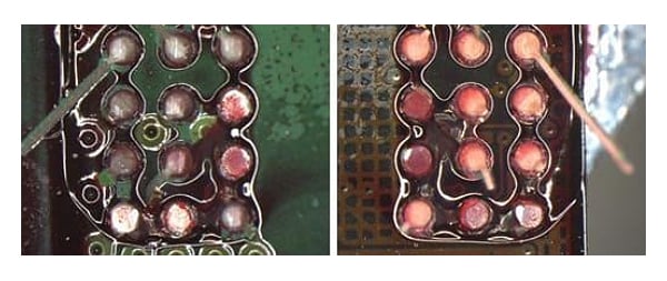
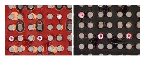
The image above shows PCB assembly defects, where red dye is visible, revealed by Covalent dye and pry PCB solder joint crack IMC defect. The board side (left) and component side (right) show solder joint cracks at the board intermetallic (IMC) layer, a defect per IPC-A-610G, section 8.3.12, and board pad lifts (cratering), a defect per
IPC-A-610G, section 10.3.2.
The image above illustrates solder joints on the board (left) and component (right) section of the PCB, marked by red dye, indicating HiP defects. These non-continuous solder joints are defects per IPC-A-610G, section 8.3.12.
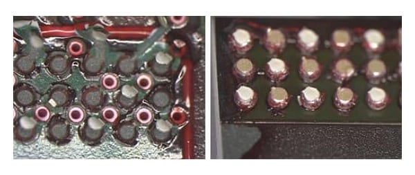
The image above indicates no pre-existing cracks or other separations on either side of the PCB. While the dye adheres to the solder balls and the solder mask windows, it does not penetrate the joints. These solder joints are acceptable per IPC-A-610G, section 8.3.12.
What we accept:
- Circuit board with BGA and SMT solder joints.
- Coating-free sample or one with coating/staking material that’s removable with standard solvents.
- Minimum size of ~1mm x 1mm, but must fit within a 12” diameter vacuum chamber. Larger boards will be cut.
Use Cases
With a focus on component-level PCB solder joints, Covalent Dye & Pry is used primarily in quality control processes in electronics manufacturing and semiconductor businesses. It’s also deployed in related industries where electronics reliability is critical, such as in aerospace, defense, telecommunications, and medical equipment companies. The service allows these businesses to reduce the negative cost, operational, productivity, and reputation ramifications of faulty circuit boards and componentry.

Electronics Manufacturing / Semiconductor/ Medical Equipment
Component integrity inspection: Evaluating the integrity of hundreds of tiny solder balls simultaneously, the service identifies ball-to-package, ball-to-pad interface, HiP, and other defects.
Aerospace & Defense
Assessing mechanical and thermal stress failures: Diagnosing failures caused by thermal cycling, thermal shock or mechanical shock and drop allows companies to make adjustments that get operations quickly back on track.
Telecommunications
Manufacturing defect inspection: Detecting issues caused by manufacturing processes, such as board flexure from de-paneling (breaking apart large printed circuit board panels), enables the timely resolution of glitches to minimize materials waste and lost production time.
Complementary Techniques
- 2D X-Ray: Used before Dye & Pry to confirm suspected defects. When the X-ray shows possible solder anomalies but lacks certainty, Dye & Pry provides visual verification before recommending any process changes.
- Mechanical Cross-Section Analysis: Used after Dye & Pry to understand why defects occur. Once Dye & Pry identifies solder joint issues, cross-sectioning a similar device reveals the root cause, such as compositional or structural problems, often confirmed through SEM/EDS analysis.
Mechanical Cross-Section Analysis (X-Section)
Uncovers microstructures and defects causing performance issues. Explore
Why Choose Covalent for Your Dye & Pry Needs?
Frequently Asked Questions
Identifying the right test can be complex, but it doesn’t have to be complicated.
Here are some questions we are frequently asked.
What package types (e.g., BGA, QFN, CSP) are compatible with Dye & Pry?
PCB solder joints formed with BGA and SMT connections are evaluated by Dye & Pry.
How does IPC‑TM‑650 specify the Dye and Pry test procedure?
IPC-TM-650 gives clear guidelines for the condition of the dye, the vacuum pressure to be used and the temperature for baking. These conditions ensure that all exposed solder defects are filled with dye and fully dried to avoid inaccurate results. The procedure also explains sample handling methods to avoid inducing damage prior to the test.
Can Covalent Dye & Pry detect voids and black pad failures in lead-free solder joints?
Dye & Pry can detect black pad failures. We can sometimes detect voids if they are very close to the joint edge and partially exposed to air. However, we would first recommend 2D X-ray as a more effective non-destructive measurement.
What sample prep steps are essential for accurate Dye infiltration?
It’s imperative to thoroughly clean the PCB with solvent to remove debris and flux residues around the solder joints. Conformal coatings or staking material must also be removed prior to dye application to allow penetration of the solder joints. PCBs that are too large to fit in the vacuum chamber will be cut with a low-vibration wire saw.
Does Dye & Pry damage the component or PCB, and can parts be reused?
Yes, the process damages the circuit board and components being tested, which typically are not reusable.
How does Dye and Pry complement X‑ray or SAM in failure analysis?
The technique dovetails with X-ray fault analysis techniques, because each approach has its strengths and downsides. Where dye and pry relies on destructive analysis, for example, X-ray is a non-destructive process. However, where X-ray can’t detect fine cracks and craters, Dye and Pry can. For its part, scanning acoustic microscopy (SAM), like X-ray, is a non-destructive testing technique. It uses high-frequency sound waves (ultrasound) to create images of the internal structure of a component. Its strength is in detecting interfacial defects and its ability to find “air-gap” defects, such as delamination.This makes it an effective process before using dye and pry to search for defects in the solder joints between component and PCB.
What turnaround time does Covalent offer for Dye & Pry services?
The standard Covalent Dye & Pry turnaround time is 5-7 business days.
Can Dye & Pry be used to inspect hidden solder joints under conformal coating?
No. Conformal coating acts as a liquid barrier and will prevent the dye from penetrating the solder joints. If conformal coating is present, we will remove it with solvents before dye application.
How detailed are the inspection reports? Do they include imagery and failure mapping?
Covalent inspection reports always include high-resolution, stitched images of the entire component area on both the component and PCB side. We provide zoomed-in images of observed dye penetration, with the locations marked on the overall image. Results summaries are dependent on your needs. Simplified results provide approximate frequency distributions of the separation interfaces, with a count of dye-penetrated solder joints and the marked locations. A more detailed summary includes maps of both separation interface and dye penetration locations, including percentage coverage of the dyed solder joint. No matter what, dye penetration will always be documented and presented front and center.

Resources