What Is Scanning Acoustic Microscopy (SAM)?
Scanning acoustic microscopy (SAM) is a non-destructive failure analysis technique that uses ultrasound reflection echoes to image internal part defects such as cracks, voids, delamination, and inclusions.
Other Details:
- Pinpoint defects early to reduce costly product recalls.
- Enables rapid defect screening for large sample batches.
- Enhances supplier audits with objective defect data.

High‑Resolution
Imaging
Measurement Principle
Uses ultrasound reflection echoes with A-, B-, and C-scan modes to image internal cracks, voids, delamination, and inclusions.

Resolution and
Sensitivity
Resolution and
Sensitivity
Frequency-dependent lateral resolution down to 5–10 µm at 200+ MHz; axial detects 10–100 nm air pockets.

Analytic Capability
Analytic Capability
Time-of-flight converts echo time to thickness, enabling bond quality assessment, layer analysis, and defect sizing.
Why Use SAM?
High-Level Advantages:
- SAM allows for internal inspection without destroying the sample.
- Provides sub-surface imaging and is capable of detecting defects below the surface, including voids, delamination, cracks, and inclusions that cannot be seen optically.
- High-resolution imaging enables the precise localization of internal features of flaws and their specific characteristics. Additionally, individual layers can be analyzed at high resolution, allowing multiple layers to be investigated in a single session.
- Minimal sample preparation beyond basic maintenance of the sample holder, which is done regularly, results in a short analysis time and high throughput.
- Failure Analysis: SAM aids in sourcing root causes of failures in a variety of materials (including those encased in plastic, circuit boards, and silicon wafers).
- It can be used as an in-line QC metrology to assess the integrity of materials, including specific components such as coatings, sealing, and underfills.
Industries that benefit from this technique:
- Semiconductor and electronics: Delamination, void, and cracking detection, quality verification of components, ICs, bond layers, and warpage.
- Material science and research: Characterization of composite materials, inspection of ceramics and polymers, multilayer structure imaging, thickness mapping.
- Medical devices: Inspection of internal air bubbles, verification of encapsulant quality, and assessment of adhesive throughout devices.
- Automotive and aerospace: Assess braze quality, weld joints and inclusions of large-scale sheets.
Analytical Depth:
Provides imaging of internal and surface structural features; A-scan, B-scan, and C-scan modes are all used to garner depth-specific signal response for potential interpretation of layer thickness, bond quality, and defect size.
Material Compatibility:
Solid, regularly shaped, and minimally rough materials that are chemically and structurally sound in deionized water. Additionally, very soft, porous, or significantly layered materials do not provide good data as they sometimes impair sound scattering.
Spatial Resolution:
It is entirely dependent on the frequency of the transducer and the longitudinal speed of sound.
- 10 MHz 150 – 300 micron lateral resolution.
- 50 MHz 20 – 50 micron lateral resolution.
- 200 + MHz 5 – 10 micron lateral resolution.
- Axial resolution -> 10-100 nm thick air pocket.

High Throughput QC
Minimal sample preparation and rapid scans enable fast defect screening across large batches with automated recipes.

Layer-Specific Insight
C-scans at multiple focal depths profile individual layers to localize delamination, voids, and cracks.

Broad Material Coverage
Non-destructive internal inspection across plastics, circuit boards, silicon wafers, composites, ceramics, and polymers.

Working Principle
Scanning Acoustic Microscopy operates by sending high-frequency ultrasound into a sample and capturing the reflected echo signals from internal interfaces and defects. A‑scan, B‑scan, and C‑scan modes are used together to collect depth‑specific signal responses that can be interpreted for layer thickness, bond quality, and defect size. Time‑of‑flight measurements convert echo travel time into distance or thickness, enabling surface warpage mapping and quantitative thickness analysis. C‑scans at multiple focal depths provide layer‑by‑layer profiling, while overall detection is constrained by sample size limits (up to 670 mm × 560 mm × 70 mm) and the tradeoff between frequency and penetration depth, where the highest‑resolution images are limited to more surface‑level layers.
Equipment Used for SAM:
PVA TePla SAM 501 HD
- Frequency Range: 1 MHz – 400 MHz.
- Lateral Scan Range: 510×510 mm.
- Vertical Scan Range: Up to 500 mm.
- Minimum Pixel Size: 0.5 µm.
- Delamination Detectability: 0.5 µm.

PVA TePla SAM 302 HD2
- Frequency Range: 1 MHz - 400 MHz.
- Lateral Scan Range: 320 mm x 320 mm.
- Vertical Scan Range: Up to 320 mm.
- Minimum Pixel Size: 0.5 µm.

Key Differentiators
This service delivers high-resolution, layer-specific imaging with minimal sample preparation. It is a versatile and relatively fast non-destructive imaging technique to identify defects in a variety of material types and sample geometries. Because of this, we serve a variety of industries, including semiconductor, battery, automotive, and biomedical industries.
Strengths
- High penetration depth enables visualization of the underlying and internal structures.
- Able to characterize buried topographies that are difficult or impossible to resolve with other microscopy techniques.
- Non-destructive analysis, however, the sample will get wet.
- Layer-specific imaging makes this technique ideal for analyzing multi-layered materials in isolation.
- Minimal sample preparation and changes were made to the samples generally.
- Access to a wide range of transducers 2.5 MHz – 250 MHz. GHz is possible but requires method development and is limited to certain sample types.
Limitations
- Limited penetration depth: Typically limited to a few millimeters, although this decreases as frequency increases. Frequency (which leads to higher resolution) and depth of penetration are inversely related.
- Water coupling requirement: Samples must get submerged in water for SAM to work properly, which is not ideal for porous or water-sensitive materials.
- No elemental and chemical information; SAM focuses entirely on physical and structural characteristics and provides no data regarding compositional information.
- Requires reasonably flat surfaces (although leveling can be done to ensure slanted surfaces are topographically flat); however, topographically flat surfaces can be properly analyzed. However, irregular or rough surfaces can scatter sound and negatively affect data collection, leading to lower image quality.


Unsure Whether SAM Is Right for You?
Learn how Scanning Acoustic can give you non-destructive, high-resolution imaging of sub-surface defects and bond quality.
Sample Information
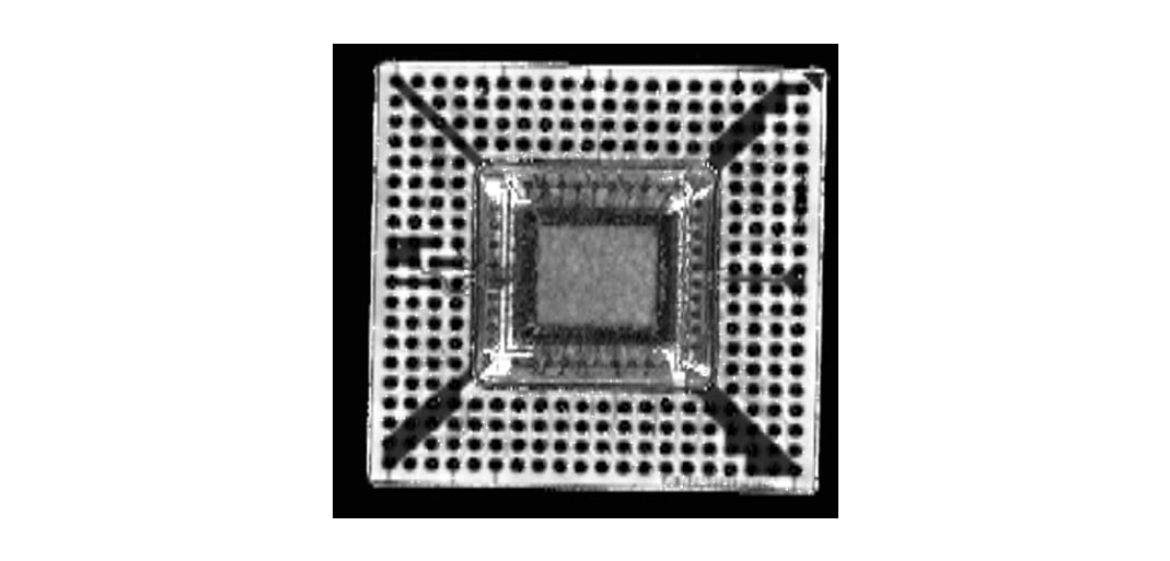
CSAM image of the solder ball-substrate interface of a flip chip.
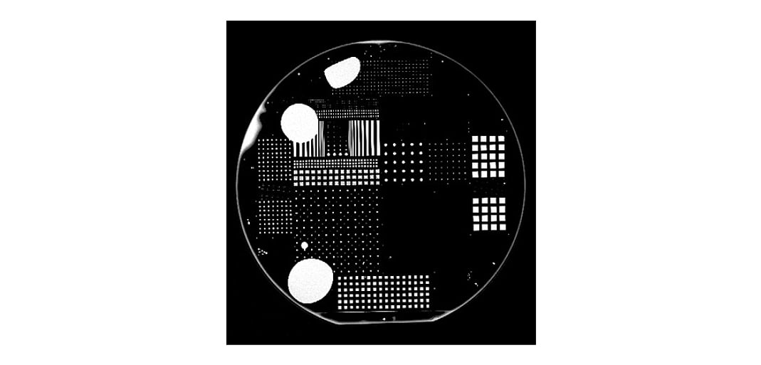
CSAM image of a bonded wafer. Large voids and delamination can be readily seen.
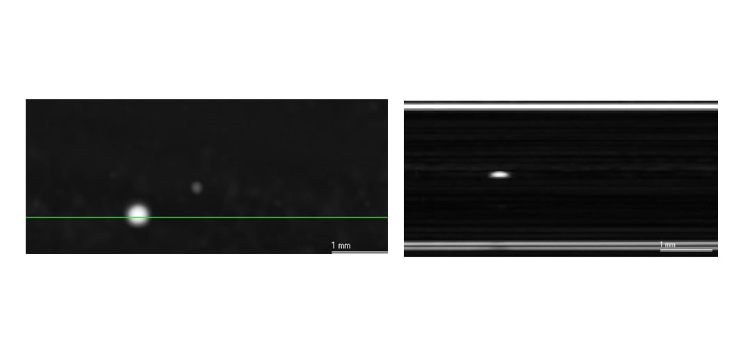
C-scan and subsequent B-scan (cross-sectional image) of an inclusion in a steel plate. We can use the B-scan image to locate how deep the inclusion is from the top surface.
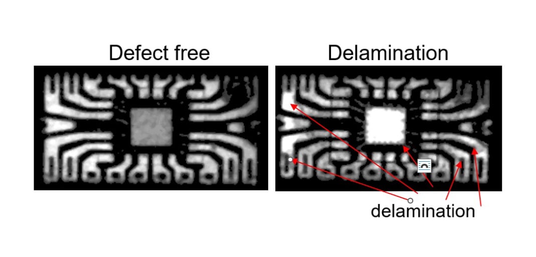
Delamination appears as bright areas.
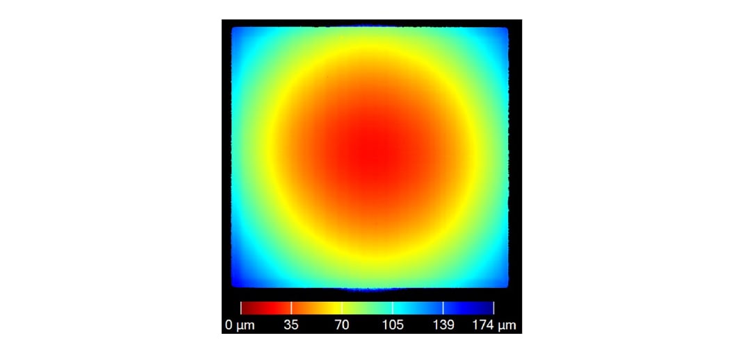
Time-of-flight (ToF) measures surface warpage. This mode can also be used for thickness mapping. ToF uses the amount of time needed for the reflected echo signal to travel from the transducer to the interface surface. Using the speed of sound of the material the echo signal is transmitting through, then the time can be converted to distance or thickness.
What we accept:
- Physical form: Solid, flat surfaces with minimal roughness (roughness disrupts signals). In some cases, a rotational gimbal can be used for scanning curved surfaces such as rods, chucks, tubes, and cones.
- Necessary properties (e.g., volatility, thermal stability): Dimensionally stable and will not degrade in water. Samples must be minimally volatile so as not to form signal-disrupting bubbles during scanning. All surface adhesives and coatings must be fully dried prior to analysis.
- Sample size: Maximum is 670 mm x 560 mm x 70 mm.
Use Cases

Manufacturing
In MEMS fabrication & packaging, SAM (especially high-frequency modes) localizes delamination, voids, and micro-cracks (down to \~40 nm scale) in ASIC surfaces and bonded wafers, helping manufacturers improve device reliability.

Medical Imaging
Producers of medical imaging probes utilize SAM to inspect multilayer structures and bonding layers, identifying defects quickly (often within minutes) and enabling root cause analysis of bond line failures, blisters, or irregular adhesive thicknesses during manufacturing.
Microelectronics
In packaging plastic ICs, flip-chips, bonded wafers, or printed circuit boards, SAM reveals subsurface defects like voids, delamination, or adhesion faults, supplementing optical & IR microscopy to ensure integrity before final assembly.
Aerospace & Materials Science
Research and industry use SAM for detecting hidden defects, internal stress anisotropy, and delamination in composites, ceramics, and
non-transparent hard materials in aerospace and structural applications.
Complementary Techniques
- Focused Ion Beam Cross-Sectioning (FIB): FIB uses a focused ion beam (typically gallium) to precisely image samples at the nanoscale by interacting with the sample to cause material removal or deposition while imaging the new exposed area. If samples can be altered, destructive cross-sectioning enables nanometer-scale imaging of defects, allowing for direct visualization using SAM.
- Optical microscopy/IR microscopy: Optical microscopy can provide high-resolution surface imaging, and IR imaging can provide contrast in materials at and below the surface. These are ideal for layer thickness, bond line visibility, and surface contaminant detection and can be used prior to SAM for any contaminants that might impair SAM accuracy. Additionally, IR microscopy can sometimes image through encapsulants where SAM is blocked.
- Scanning Electron Microscopy (SEM): If samples can be altered, SAM can first be used on whole samples to locate internal defects, and then sectioning of samples to image those regions with SEM will provide information regarding specific morphological features.
- X-ray Computed Tomography (Micro-CT): Where SAM offers images at specific, defined interfaces, micro-CT provides data regarding total internal structure, complementing SAM by providing information regarding internal geometries, including voids, at deeper levels than SAM can reach.
- X-ray Radiography (2D X-ray): Quick, 2D imaging of internal structures to provide information regarding gross defects, which can then be analyzed using SAM for more specific, high-resolution images.
Scanning Electron Microscopy (SEM)
Images surface topography and composition with electrons. Explore
X-ray Computed Tomography (Micro-CT)
Non-contact, non-destructive 2D/3D images at micron scale. Explore
Why Choose Covalent for Your SAM Needs?
Frequently Asked Questions
Identifying the right test can be complex, but it doesn’t have to be complicated.
Here are some questions we are frequently asked.
How long does a typical acoustic microscopy analysis take?
Setting up a recipe can take 1-3 hours, but once a recipe is established, then it can take only a few minutes per scan.
What is the cost range for SAM testing for small vs large samples?
We can batch small samples on a tray and perform automated scan recipes. Therefore, after a recipe is established, small samples can be $100-$200/sample depending on the number of samples provided.
What is the minimum defect size reliably detected for various materials?
This depends on the speed of sound of the material and the frequency. For a material like silicon with a 200 MHz transducer, the lateral resolution is about 8 microns.