What Is Spectroscopic Ellipsometry (SE)?
SE measures how the polarization of light changes as it reflects from or transmits through a sample, providing information about film thickness, refractive index (n), extinction coefficient (k), and other optical constants.
SE is most often used when other methods, such as profilometry (which requires step edges) or reflectometry (often limited to only thickness measurement), cannot simultaneously determine both thickness and optical properties with the same level of accuracy. This makes SE especially valuable for complex multilayer stacks, semiconductor coatings, and thin dielectric or polymer films where material properties and layer uniformity are critical.
Other Details:
- Covers a broad spectral range (193 nm–35 µm) and film thickness range (1 Å–25 µm+).
- Advanced modeling resolves complex multilayer stacks with high precision.
- Compatible with dielectrics, metals, semiconductors, polymers, and more.
- Automated mapping stage enables high-resolution uniformity measurements across large wafers.

Speed and Efficiency
Speed and Efficiency
Single measurements can be collected in less than a second.

Exceptional Precision and Accuracy
Exceptional Precision
and Accuracy
For high-quality films, SE can achieve 0.1% precision and approximately 1% accuracy.

Non-Destructive Testing
Non-Destructive Testing
The measurement process does not alter or damage the sample, preserving its integrity for further testing or use.
Why Use SE?
- Greater sensitivity to film thickness and refractive index (n) than other common optical methods.
- Can deconvolve individual layers in multilayer stacks more effectively.
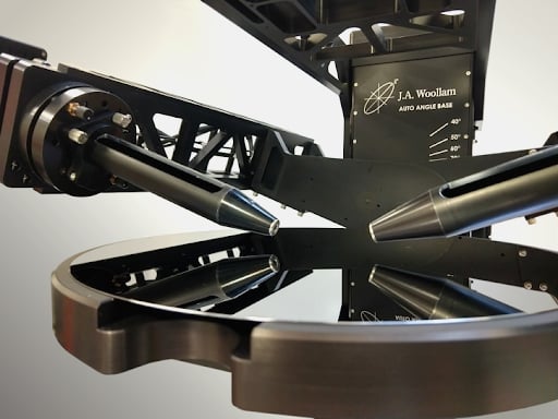
- Covalent’s state-of-the-art J.A. Woollam RC2 ellipsometer is fast, precise, and flexible.

Analytical Depth
SE analyzes surface and subsurface layers, inferring thickness, optical properties, interfacial mixing, and bandgap.

Material Compatibility and Sample Size
SE can measure nearly all materials, including dielectrics, semiconductors, metals, polymers, and more, in both thin film and bulk form for samples spanning sizes from ~1 to 300 mm.

Depth Profiling
SE excels at measuring multilayer stacks and can sometimes detect depth-dependent optical or compositional changes.
Working Principle
A polarized light beam reflects from the sample, and changes in polarization amplitude and phase are recorded across multiple wavelengths. These changes are modeled to extract film thickness and optical constants (n, k) with high precision.
Equipment Used for SE:
At Covalent, we use the J.A. Woollam RC2-DI, a highly advanced spectroscopic ellipsometer for precise optical analysis.
J.A. Woollam RC2-DI
- Spectral Range: 193 to 1690 nm (0.73 to 6.42 eV; 1075 total wavelength bands).
- Dual-rotating compensator configuration (PCRSCRA configuration).
- Automated mapping up to 300 mm substrates w/ fully customizable X-Y resolution and scan pattern.
- Measurement Beam Diameter: 5 mm (standard); or 300 µm (focused).
- Full Muller matrix measurement capability.
- Variable-angle transmission stage (45° – 90° angle-of-incidence range).
Key Differentiator
Delivers precise, non-contact measurement of film thickness and optical properties-beyond the limits of reflectometry or profilometry.
Strengths
- Wide spectral (193 nm–35 µm) and thickness (1 Å–25+ µm) range.
- Quick, non-contact measurements, often under 10s.
- High precision: <0.1% repeatability, ~1% of true value.
- Advanced modeling resolves complex multilayer stacks.
Limitations
- Requires smooth, flat samples for accurate results.
- Cannot measure opaque or deeply buried layers.
- Development of optical models can be time-consuming for complex projects.


Unsure Whether SE Is Right for You?
Find out whether SE is the best choice for your complex multilayer films, from semiconductor coatings to dielectrics and polymers, with practical recommendations tailored to your sample.
Sample Information
Raw spectroscopic ellipsometry measurement data are changes to the polarization state of light when reflected off a sample. The final experiment outputs are obtained by fitting optical models to the raw data to extract meaningful material properties, such as thin film thickness, optical constants, and more. The figures below provide illustrative examples of results from ellipsometry measurements.
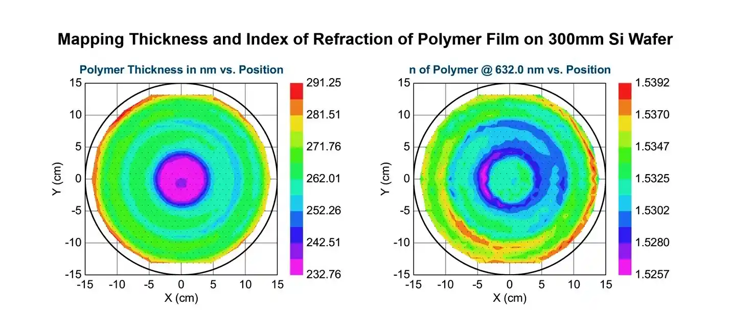
The output above shows two high-resolution spatial maps of a polymer thin film deposited on a 300mm Si wafer. The figure on the left maps the variation of the polymer’s layer thickness, while the figure on the right maps the variation of the polymer’s index of refraction. While the variations in the film have angular symmetry, there are substantial variations in the film thickness and index of refraction as a function of radial position.
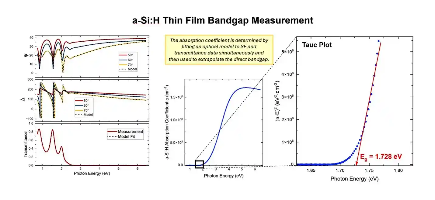
The output above illustrates a measurement of an a-Si:H thin film bandgap. An a-Si:H thin film deposited on glass is measured using reflection SE and unpolarized transmittance (%T). The left figure shows the result of fitting an optical model (represented by dotted black lines) to both sets of the SE and %T data simultaneously. Fitting to both data types allows maximum accuracy of the a-Si:H absorption coefficient, plotted in the center figure. Finally, in the figure on the right, a Tauc plot is made from the data at the absorption onset. The bandgap is extracted by fitting the data’s lowest approximately linear portion, as shown by the red linear fit line. The bandgap of this a-Si:H film is determined to be 1.728 eV.
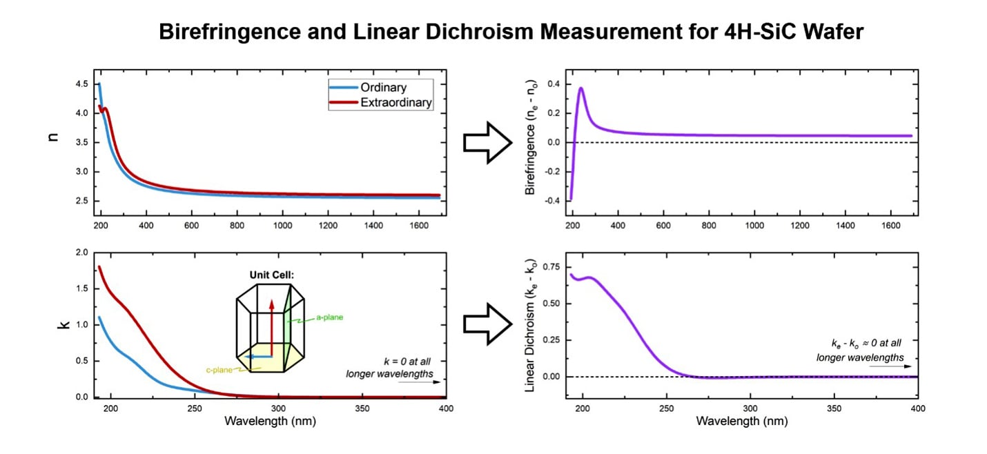
The images above show measurements of the uniaxially anisotropic optical properties of a c-plane 4H-SiC wafer using Mueller Matrix SE. The figures on the left plot the resulting index of refraction (n) and extinction coefficient (k) for this sample, where the optical properties differ along the two crystallographic axes. The right plots show the birefringence and linear dichroism, which are calculated as the spectroscopic index and extinction coefficient differences, respectively.
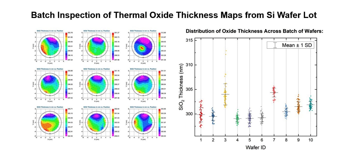
The figures above reflect a cassette of Si wafers, each with a thermal oxide surface film, mapped to measure the spatial distribution of thermal oxide thickness. The figure on the left shows the resulting spatial thickness maps for nine of these wafers. The thickness data from each wafer is plotted and compared in the distribution summary plot on the right, which enables a statistical understanding of variation in oxide thickness across the full lot of wafers.
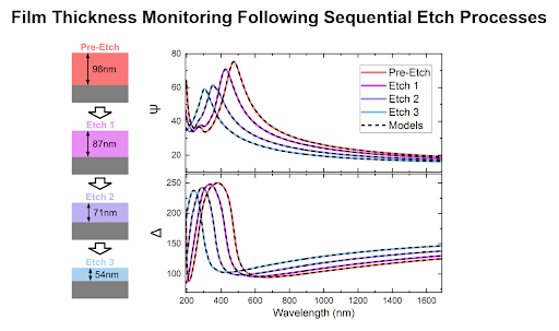
The output above demonstrates SE monitoring the progressive decrease in film thickness following repeated etching processes. The left schematic shows the thickness results following each etch, and the figure on the right shows the model fit to the measured SE data for measurements collected after each etch. These high-precision results help tune the etching process parameters to achieve fine control over the resulting film thicknesses.
What we accept:
SE works best on flat, smooth samples. Sizes range from 1 mm to 300 mm, and film thicknesses range from 1 Å to 25+ µm. Films must be at least partly transparent to measure thickness. For multilayer stacks, a single SE measurement can typically only measure 2 unknown materials at once. Film stacks with many unknown layers typically require intermediate samples with partial stacks.
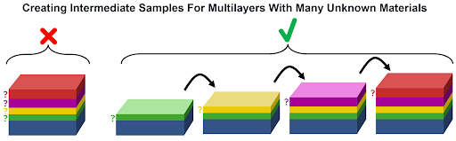
The image above, left, illustrates that it is typically not feasible to accurately determine properties of all layers from a single SE measurement of the whole layer stack. The schematic on the right shows the widely preferred method of creating a series of multiple partial-stack samples, where each sample sequentially adds another layer until the final stack is complete. Measuring each of these samples and modeling them sequentially results in the most accurate and unambiguous results, because each measurement is only responsible for determining properties of a single layer at a time.
Use Cases

Semiconductor & Microelectronics
SE is essential in microelectronics, characterizing dielectrics, metals, and semiconductors. It precisely measures complex film stacks and helps monitor and optimize deposition and etch processes.

Energy
SE is ideal for photovoltaic (PV) applications, measuring bandgap, layer and interface thickness, and optical absorption in semiconductor absorbers and transparent conducting oxides. It also maps large-area uniformity critical to PV fabrication.
Display & Optoelectronics
SE enables precise analysis of thin film stacks that form the base of displays and sensors. It accurately measures optical coatings, color filters, and absorber layers used in optoelectronic devices.

Biomedical
SE is one of the few techniques capable of measuring ultra-thin self-assembled monolayers (SAMs) and silanized surfaces. It’s also well-suited for characterizing hydrogels, parylenes, PEG, fluoropolymers, and polymer brushes.
Polymers
SE characterizes optical properties, thickness, and surface gradients in polymer films, helping assess curing behavior, optical uniformity, and coating coverage.
Complementary Techniques
- FTIR Transmittance Spectroscopy: Used to enhance sensitivity to fine absorption features in the infrared spectrum, extending SE’s sensitivity in this range.
- Transmission Electron Microscopy (TEM): Used to obtain high-resolution nanoscale cross-sectional images for verifying and validating SE optical models of multilayer structures.
- UV-Vis-NIR Spectrophotometry: Transmittance and reflectance data are frequently modeled together with SE data to enhance sensitivity to low values of the extinction coefficient inaccessible to just reflection SE alone.
- X-ray Photoelectron Spectroscopy (XPS): Used to quantify surface oxide thickness (up to 10 nm) and composition on metals for use in calibrating SE models.
- X-ray Reflectivity (XRR): Used for dense or buried thin films where SE sensitivity decreases.
Fourier Transform Infrared Spectroscopy (FTIR)
Rapid, non-destructive molecular fingerprinting across materials. Explore
Transmission Electron Microscopy (TEM)
Images atomic structure, defects, interfaces with sub-nm resolution. Explore
Ultraviolet Visible Near Infrared Spectrophotometry (UV-Vis-NIR)
Measures absorbance, reflectance, and transmittance (175–3300 nm). Explore
X-ray Photoelectron Spectroscopy (XPS)
Measures surface elemental composition and chemical states. Explore
X-ray Reflectometry (XRR)
Optimized scans tailored to each sample for best measurements. Explore
Why Choose Covalent for Your SE Needs?
Frequently Asked Questions
Identifying the right test can be complex, but it doesn’t have to be complicated.
Here are some questions we are frequently asked.
How thin can a film be for accurate spectroscopic ellipsometry analysis?
If measuring thickness of a film is the measurement goal, SE can accurately measure film thicknesses as low as 1 Å as long as there is large difference in the index of refraction between film and substrate. To accurately measure both the film thickness and optical property spectra (n, k), films must be thicker, however. Although there is no absolute minimum thickness for measuring both thickness and optical properties, a good rule of thumb is that ~ 5-10 nm is about the thinnest a film could be for reasonably accurate results.
Can spectroscopic ellipsometry measure complex refractive index (n & k) across the IR spectrum?
Yes! In general, Covalent has the ability to use spectroscopic ellipsometry to measure n & k for films and bulk materials from the vacuum ultraviolet to the mid-infrared (150 nm – 35 μm). Through a combination of measurements on separate ellipsometers, each designed for a particular portion of the spectrum, we can collect a continuous spectra over this entire range and develop corresponding optical models to obtain a single continuous spectrum for both n & k over this entire range (or any subset of the full range).
What materials are suitable for infrared spectroscopic ellipsometry?
Although virtually any sample that is flat and smooth can be measured with infrared SE, the same limitations that apply to visible and UV range SE are present in infrared SE. Specifically, thickness can only be measured for films with transparency over at least part of the measured spectral range. In addition, the sample configuration will strongly influence how feasible it is to measure thickness and optical properties of materials (e.g. significant index contrast between film and substrate is desirable). In practice, infrared ellipsometry is frequently applied to dielectrics, semiconductors, polymers, and metals.
Do you support multilayer thin‑film modeling and fitting?
Yes, Covalent specializes in optical modeling of virtually any multilayer thin-film structure. If the project is possible, we almost certainly can support it. In fact, the vast majority of all optical modeling we do is customized to the specific samples and overall measurement goals.
Are your spectroscopic ellipsometry results ISO/GLP compliant?
Covalent is an ISO 17025 accredited laboratory and our spectroscopic ellipsometry work is covered under this accreditation. Additionally, we have the optional ability to collect NIST-traceable spectroscopic ellipsometry data. The scope of GLP compliance does not have strong relevance to typical projects suitable for spectroscopic ellipsometry.

Resources