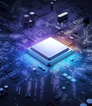
What Is Focused Ion Beam Scanning Electron Microscopy (FIB-SEM)?
FIB-SEM is a powerful analytical technique that provides detailed insights into the morphology of subsurface features, enabling visual identification of key structures and areas of interest. When combined with EDS, it allows for precise investigation of the chemical composition of specific regions. This technique is compatible with a wide range of materials, including metals, ceramics, polymers, and semiconductors, though sample preparation requirements vary depending on conductivity. FIB-SEM offers high spatial resolution, with lateral resolution reaching approximately 5–10 nm under Ga⁺ FIB conditions, and excels in depth profiling, making it ideal for layered materials analysis from nanometers to microns deep.

Resolution
Resolution
Captures nanoscale morphological details of subsurface features for precise structural analysis.

Versatility
Versatility
Compatible with metals, ceramics, polymers, and semiconductors, accommodating diverse research and industrial needs.

Composition
Composition
When combined with EDS, it enables localized elemental composition mapping alongside structural insights.
Why Use FIB-SEM?
FIB-SEM is the go-to tool for precise, site-specific analysis of micron- and submicron-scale features in devices, thin films, composites, and other materials. It enables the extraction and thinning of lamellae to electron transparency (~100 nm) for Transmission Electron Microscopy (TEM), giving nanometer-level accuracy for targeted regions. The technique combines imaging and modification in a single system, supports correlative imaging with SEM, EDS, and EBSD, works across metals, semiconductors, ceramics, polymers, and bio-samples, and enables 3D reconstruction for volumetric imaging at nanometer resolution.

Precision
Targets specific regions of interest with nanometer-level accuracy for detailed site-specific analysis.

Versatility
Supports a wide range of materials – metals, semiconductors, ceramics, polymers, and bio-samples and multiple imaging modalities.

3D Insight
Enables volumetric imaging and FIB-SEM tomography for comprehensive nanoscale structural understanding.

Working Principle
The key advantage of the FIB is its ability to selectively remove material to expose subsurface features. FIB is typically used to cross-section thin film stacks or device structures for subsequent analysis using the SEM. FIB-SEM allows for targeted material milling and sputtering on a scale of nanometers to tens of microns.
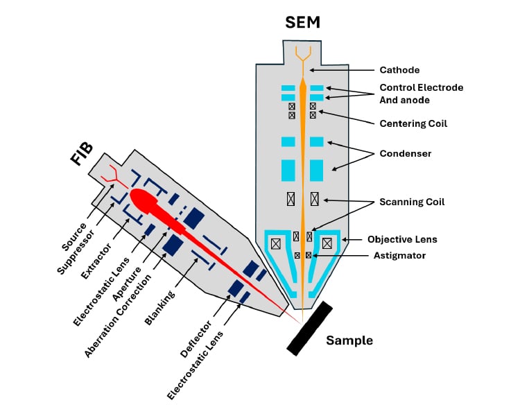
This schematic describes the major components of a focused ion beam- scanning electron microscope, dual beam system.
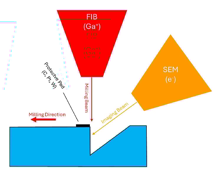
This schematic displays a transverse view of a FIB cross section where the FIB is normal to the top surface of the sample. The electron beam is imaging the cross sectioned plane at 38 degrees relative to horizontal of the sample and stage, and is 52 degrees from the FIB column
Equipment Used for FIB-SEM:
Thermo Fisher Helios 5 UC Dual Beam
- Electron beam resolution:
- At optimum WD:
- 0.6 nm at 30 kV STEM.
- 0.7 nm at 1 kV.
- 1.0 nm at 500 V (ICD).
- At coincident point:
- 0.6 nm at 15 kV.
- 1.2 nm at 1 kV.
- At optimum WD:
- UC+ monochromator.
- Ion Optics: Down to 500kV for final polishing on TEM lamella.
- Automated TEM Prep for fast/repeatable throughput: Thermo Scientific™ AutoTEM™ Software for automated STEM sample preparation.
- Sample:
- Max sample weight: 500 g (including sample holder).
- Max sample size: 150 mm with full rotation (larger samples possible with limited rotation).

Thermo Fisher Helios 6 HD Dual Beam
- New FIB column with automated source and column alignments provides increased stability and low-kV milling capabilities.
- New digital scanning and patterning engine allows for simultaneous SEM imaging and FIB milling which enables more precise end-pointing and higher productivity.
- AutoTEM 6 Software-targeted application designed to deliver the most out of the new Helios 6 HD FIB-SEM’s hardware platform. This AI-enabled software automatically aligns all grid/finger locations, offering enhanced grid management capabilities and a decrease in set-up time.
- Longer interval between EasyLift NanoManipulator needle exchanges and streamlined replacement, leading to increased system availability and consistent results.

Key Differentiators
Strengths
- Fine details in surface topography, such as texture, roughness, and microstructure, are easy to see.
- Able to view the shape, size, and arrangement of particles, fibers, pores, grains, etc., due to the high magnification range and depth of field.
- Can provide precise 2D measurements of lengths, diameters, feature sizes, such as layer thicknesses, pore or particle sizes.
- Qualitative or semi-quantitative chemical composition of visible features.
Limitations
- SEM needs vacuum-stable, conductive samples.
- Magnetic materials can be analyzed with caution, using field-free observation modes. Avoid ultra-high resolution mode.
- FIB milling is incompatible with low vacuum modes.
- Spatial resolution is worse than TEM and degrades with high voltage/light elements.


Unsure Whether FIB-SEM Is Right for You?
Learn more about using FIB-SEM testing services today.
Sample Information
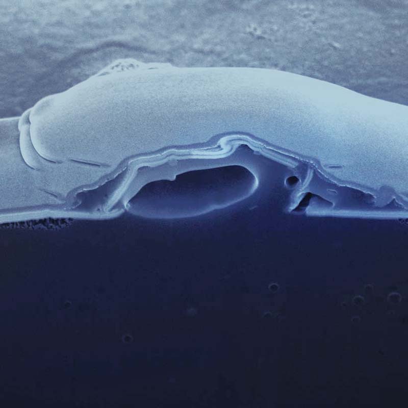
FIB-SEM cross-section of a pixel array, showing underlying nm-scale device features.
What we accept:
- Solid phase.
- Must be vacuum stable.
- Maximum Sample Height: 55 mm.
- Maximum Sample Weight: 500 g (including sample-holder).
- Maximum Lateral Dimension: 150 mm (larger samples enabled with reduced rotation).
Use Cases
Semiconductor
FIB-SEM is often used for failure analysis and process monitoring on semiconductor samples. The FIB can be used to make cross sections on the nanoscale while SEM is used in combination with EDS to image and chemically characterize the cross section.

Materials
FIB cross-section of copper foils for EBSD analysis of the cross-section for grain size and crystallographic orientation analysis.

Battery Technology
Recurring Covalent client requires routine sample analysis of a thin film stack. Covalent has successfully optimized the FIB-SEM-EDS procedures for these samples to minimize turnaround time and deliver quality data to the client.
TEM Lamella Prep
For multiple industries, including semiconductor fabrication, semiconductor devices, data storage, IC packaging, battery, optoelectronics, coatings/thin films, life sciences, and medical devices.
Complementary Techniques
- Atomic Force Microscopy: Measures 3D nanoscale surface topography and mechanical properties, useful for nanoscale surface characterization.
- Auger Electron Spectroscopy: A surface-sensitive elemental analysis technique with high spatial resolution, ideal for interface and failure analysis.
- Fourier Transform Infrared Spectroscopy: Detects molecular bonds and chemical structures, and is ideal for contamination and surface residue analysis.
- Scanning Transmission Electron Microscopy: Provides atomic-scale resolution of internal features.
- Secondary Ion Mass Spectrometry: An elemental analysis technique with ultra-sensitive chemical and isotropic analysis, used to prepare flat or site-specific surface for high-resolution SIMS.
- Transmission Electron Microscopy: Provides atomic-resolution imaging and crystallographic detail.
- X-ray Photoelectron Spectroscopy: Provides elemental and chemical state information of the top few nanometers of the surface, ideal for surface chemistry and thin films.
Atomic Force Microscopy (AFM)
Maps nanoscale topography and material properties with a sharp probe. Explore
Auger Electron Spectroscopy (AES)
Measures Auger electrons for high-resolution surface analysis. Explore
Fourier Transform Infrared Spectroscopy (FTIR)
Rapid, non-destructive molecular fingerprinting across materials. Explore
Scanning Transmission Electron Microscopy (STEM)
Provides atomic-scale imaging and spectroscopic mapping. Explore
Transmission Electron Microscopy (TEM)
Images atomic structure, defects, interfaces with sub-nm resolution. Explore
X-ray Photoelectron Spectroscopy (XPS)
Measures surface elemental composition and chemical states. Explore
Why Choose Covalent for Your FIB-SEM Needs?
Frequently Asked Questions
Identifying the right test can be complex, but it doesn’t have to be complicated.
Here are some questions we are frequently asked.
What is FIB-SEM used for?
FIB-SEM (Focused Ion Beam – Scanning Electron Microscopy) is a powerful dual-beam instrument for microscale and nanoscale imaging, material modification, and analytical characterization. It combines the capabilities of a scanning electron microscope (SEM) for high-resolution imaging with a focused ion beam (FIB) for site-specific milling, deposition, and sample preparation.
How do you interpret FIB-SEM images?
Interpretation of SEM images of FIB cross sections relies on understanding how different contrast mechanisms relate to sample features, beam settings, and detector types. For topographic contrast using secondary electrons, bright areas are the sample’s regions facing the detector, whereas dark areas are recessed or shadowed. This allows one to identify cracks, voids, fibers, surface roughness, and 3D surface shapes. For compositional contrast using backscattered electrons, bright areas are higher atomic number elements, and darker areas are lower atomic number elements (gold vs carbon). This type of contrast allows one to identify inclusions, multi-phase materials, contamination, and coating layers. Be sure to pay attention to the scale bar when comparing the relative sizes of features in the SEM image of a FIB cross-section. When measuring the length of a vertical feature in a FIB cross-section (i.e., thin film thickness), it is essential to know the stage tilt at which the image was collected (typically 52 degrees). When using the horizontal scale bar when measuring the thin film thickness, one must multiply that value by the cosine of the complementary angle (i.e., cosine(38 degrees)) to calculate the film thickness.
What level of resolution can FIB-SEM achieve?
Under high-resolution conditions with a Ga⁺ focused ion beam (FIB), the best lateral resolution is ~5–10 nm. For imaging, a field emission scanning electron microscope (SEM) can reach sub-nanometer spatial resolution in ultra-high resolution mode.
Which industries commonly use FIB-SEM for failure analysis or microfabrication?
FIB-SEM is widely used in semiconductors, microelectronics, batteries, and the energy industry for precise cross-sectioning, defect analysis, and microfabrication.
What elemental sensitivity can be achieved with EDS in FIB-SEM?
Energy Dispersive X-ray Spectroscopy (EDS) in FIB-SEM is semi-quantitative and accurate within 0.1 weight percent. However, EDS cannot detect H, He, or Li with most detectors, and sensitivity to light elements (B, C, N, O) is reduced due to low X-ray yields and overlaps.
How is beam-induced damage minimized during FIB-SEM analysis?
Beam damage can be minimized by lowering beam energy and current to reduce the dose. This approach applies to both the electron beam and the focused ion beam, making it essential for analyzing sensitive samples.
What are the advantages of integrating EBSD or EDS with FIB-SEM?
Integrating EDS provides localized chemical composition analysis of cross-sectioned regions, enabling material identification of subsurface features. EBSD (Electron Backscatter Diffraction), under specialized conditions, can be combined with FIB-SEM for localized crystallographic mapping, revealing grain boundaries, phase orientation, and texture.
When should FIB-SEM be used instead of traditional SEM or TEM?
FIB-SEM is necessary when subsurface features must be accessed. Traditional SEM is surface-limited, while FIB enables precise cross-sections. FIB-SEM is also used to prepare TEM lamellae. TEM areas are typically 5–10 µm wide and only a few microns deep, while FIB-SEM cross-sections can reach up to 100 µm wide and tens of microns deep.
What are the sample preparation requirements for FIB-SEM analysis?
- Metals: Minimal preparation needed due to high conductivity.
- Ceramics/Polymers: Often require thin conductive coatings and grounding layers to avoid charging.
- Semiconductors: Can often be analyzed at low voltages without coating, but coatings are usually required when devices or passivation layers are present.
Good sample conductivity is critical. Non-conductive or unstable samples may drift or accumulate charge, reducing cross-sectioning accuracy.
What are the limitations of FIB-SEM for material analysis?
- Vacuum requirement: Samples must be vacuum-stable; liquids or volatile materials are not compatible.
- Resolution: Lower than TEM; worsens with beam broadening at high voltages or in low-Z materials.
- EDS sensitivity: Cannot measure H, He, or Li; reduced accuracy for light elements.
- Sample sensitivity: Biological and organic materials may degrade under beam exposure.

Resources