
What We Offer
- R&D support and process development for new materials, coatings and assembly processes
- Failure analysis of devices, PCBAs and components
- Solder joint, via and package inspection
- Display, glass and coating analysis
- Battery materials and cell teardown analysis
- Contamination and residue identification
- Material and supplier qualification
Why Teams Choose Covalent
Speed
X-ray, CT, acoustic microscopy, cross-sectioning, SEM and surface chemistry are under one roof, so a failed device goes from inspection to root cause with one team.
Quality
Nondestructive inspection comes first, so cracks, voids and delamination are found before any cutting.
Detailed reporting
Annotated images and data, followed by a results call to agree next steps.
Why Materials Analysis Matters in Consumer Electronics
Devices pack many materials into tight spaces and face heat, humidity, drops and daily wear. New materials and fast product cycles bring new failure modes. Materials analysis finds weak points early, explains field returns and keeps product quality steady as suppliers change.
Common Challenges We Solve
| Challenge | What we measure | Techniques |
|---|---|---|
| Solder joint and board failures | Cracks, voids, intermetallics, opens and shorts | 2D X-ray, micro-CT, cross-sections, SEM-EDS, dye and pry |
| Delamination in packages and displays | Hidden voids and interface separation | Scanning acoustic microscopy, cross-sections |
| Thermal mismatch | CTE and warpage of boards and packages | TMA, DSC |
| Coatings and surface finishes | Thickness, roughness, adhesion, scratches | White light interferometry, LSCM, nano scratch, XPS |
| Contamination and corrosion | Flux residue, ionic contamination, corrosion products | FTIR, ion chromatography, SEM-EDS, ToF-SIMS |
| Battery swelling and failures | Gas, electrode damage, internal structure | Micro-CT, GC-MS, SEM |
How We Work With You
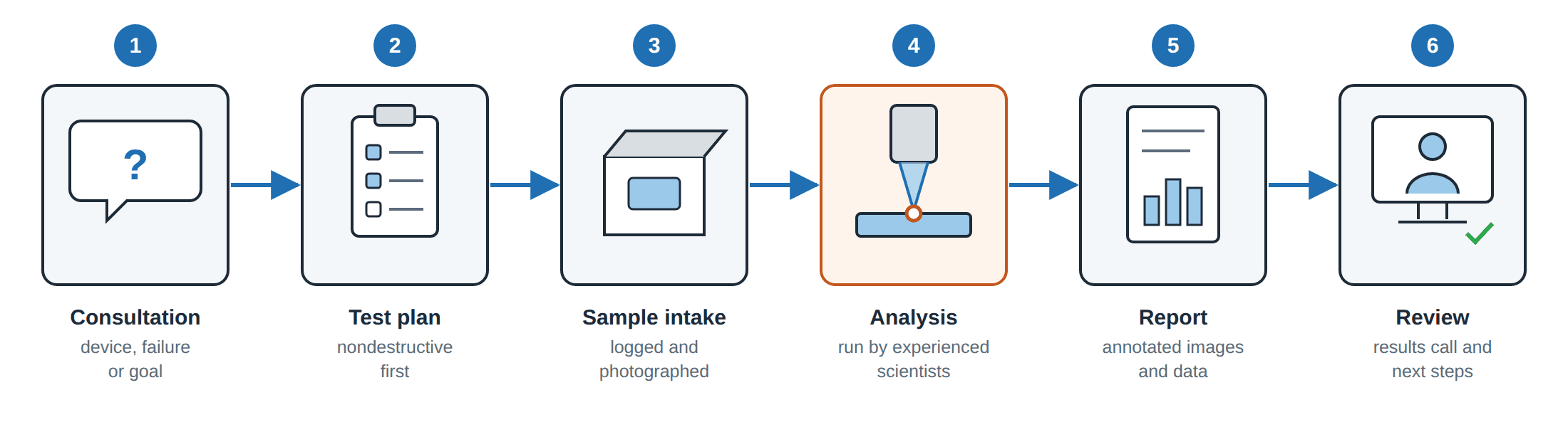
- Consultation: the device, the failure or goal, and your timeline.
- Test plan: techniques chosen for the question, nondestructive first.
- Sample intake: logged and photographed on arrival.
- Analysis: by experienced scientists.
- Report: annotated images and data.
- Review: a results call and next steps.
Techniques for Consumer Electronics Analysis
| Area | Techniques | What you learn |
|---|---|---|
| Nondestructive inspection | 2D X-ray, micro-CT, scanning acoustic microscopy | Voids, cracks and delamination inside boards and packages |
| Cross-sections and microscopy | Mechanical cross-sections, SEM, FIB-SEM, optical microscopy | Layer thickness, solder joints, vias and defects |
| Structure | XRD | Crystal structure and stress in components and battery materials |
| Surface and optical | White light interferometry, LSCM, digital optical microscopy | Roughness, topography and coating thickness |
| Thermal | TMA, DSC, TGA | Expansion, Tg and thermal stability |
| Electrical | 4-point probe, nanoprobing | Sheet resistance and device-level electrical behavior |
| Chemistry | FTIR, SEM-EDS, XPS, ion chromatography | Residues, corrosion and contamination |
| Board reliability | Dye and pry, IPC compliance testing | Solder joint cracking and IPC conformance |
From R&D to Production
- R&D and material selection: compare candidate plastics, metals, glass and coatings.
- Process development: measure how changes to bonding, coating or assembly processes affect boards and components.
- Component and material qualification: check that parts and materials meet specifications.
- Post-stress analysis: examine devices after drop, thermal or humidity testing run elsewhere.
- Manufacturing QA: verify consistency across lots and suppliers during ramp.
- Failure analysis: find the root cause of returns and field failures.
Enterprise Metrology Solutions for Consumer Electronics
Device brands and their suppliers bring Covalent's scientists into each product cycle: material and supplier selection, prototype evaluation and failure analysis of returns. One team handles inspection, cross-sections and chemistry, so you don't coordinate several labs.
Experts on your team
A technical lead and scientists who join your product and reliability reviews and know your devices, suppliers and earlier returns.
Methods development
New methods for new materials, coatings, displays and assembly processes in each product generation.
Lab on demand
Extra inspection and failure analysis capacity during a launch, a supplier change or a spike in returns.
One partner, secure data
Inspection, cross-sections and chemistry in one lab, plus Covalent Connect partner labs, under ISO/IEC 17025 and SOC 2, with results in a secure portal.
Consumer Electronics Testing Services at Covalent
Our Sunnyvale lab brings X-ray, CT, acoustic microscopy, cross-sectioning, SEM and surface chemistry under one roof, so a failed device can go from inspection to root cause with one team. Our experts help you choose the right tests, interpret the results and make data-driven improvements. For techniques we don't run in-house, we can place work through Covalent Connect, our network of trusted partner labs.
Turnaround is typically 5–7 business days, with rush options available at an extra cost.
Frequently Asked Questions
Can you find why a board failed without destroying it?
Do you offer IPC compliance testing?
Yes. See our IPC Compliance Testing page.
Do you run drop, water-resistance or EMI testing?
Can you analyze a swollen battery?
Can you identify residues on a circuit board?
Yes. FTIR, ion chromatography, SEM-EDS and ToF-SIMS identify flux residue, ionic contamination and corrosion products.
How do you protect our data and IP?
Covalent is ISO/IEC 17025 accredited, holds a SOC 2 examination and is ITAR registered. We sign NDAs, and results are delivered through a secure portal.
How quickly will we get results?
Turnaround is typically 5–7 business days, with rush options available at an extra cost.