
What We Offer
- R&D support and process development for new films, stacks and materials
- Failure analysis and defect characterization to improve yield
- Contamination control on wafers, chemicals and process tools
- Packaging and reliability analysis, from wire bonds to hybrid bonding
- Quality assurance and supplier qualification for incoming materials
Why Teams Choose Covalent
Speed
We prepare dozens of FIB lamellae every day, and fault localization, cross-sections and TEM run in one lab, so samples never ship between vendors.
Quality
Scientists with advanced degrees run each analysis, moving from nondestructive to destructive methods so the failure site is preserved.
Detailed reporting
Annotated images and data in your secure portal, then a review with the scientist who ran the work.
Why Materials Analysis Matters in Semiconductors
A chip goes through hundreds of interdependent process steps. One nanometer-scale defect, a trace metal on a wafer or a drift in film thickness can cut yield or cause field failures months later. Characterization finds those problems at the atomic scale, tightens process windows and gives you evidence to qualify designs and suppliers.
Common Challenges We Solve
| Challenge | What we measure | Techniques |
|---|---|---|
| Shrinking features and high density | Defects and dimensions in logic, memory and power devices | FIB-SEM, TEM, STEM-EDS/EELS |
| Thin films and interfaces | Thickness, composition, intermixing, roughness | XPS depth profiling, SIMS, XRR, ellipsometry, AFM |
| New channel and device materials | III-V, 2D materials, high-k dielectrics, SiC and GaN | TEM, XRD, Raman, PL, CL |
| Dopants and electrical behavior | Dopant profiles, carrier distribution, junctions | Dynamic SIMS, SCM, nanoprobing, 4-point probe |
| Trace contamination | Metals and organics on wafers and in chemicals | VPD-ICP-MS, TXRF, ToF-SIMS, ICP-MS |
| Lithography materials | Photoresists and masks, residues and defects | ToF-SIMS, PiFM, SEM, AFM |
| Packaging and heterogeneous integration | Voids, delamination, cracks, solder and bond integrity | 2D X-ray, micro-CT, SAM, cross-sections, FIB-SEM |
How We Work With You
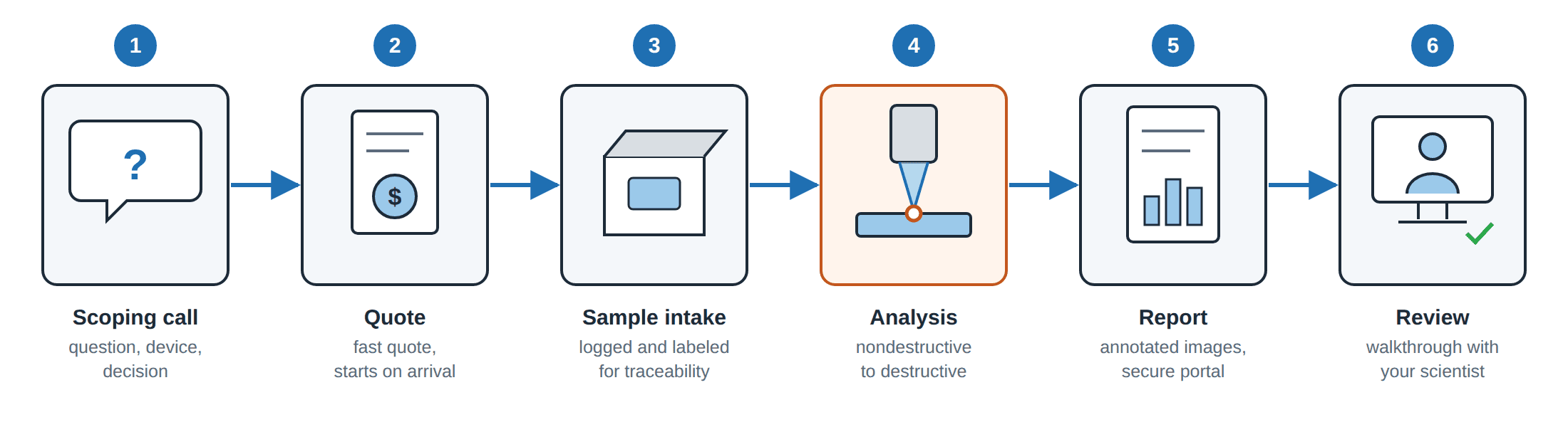
- Scoping call: we define the question, the device and the decision you need to make.
- Quote: you get a quote quickly, and work starts as soon as samples arrive.
- Sample intake: samples are logged and labeled for traceability.
- Analysis: scientists with advanced degrees run the work, moving from nondestructive to destructive methods.
- Report: annotated images and data in your secure customer portal.
- Review: the scientist who ran the work walks you through the results.
Techniques for Semiconductor Analysis
| Area | Techniques | What you learn |
|---|---|---|
| Electron microscopy | SEM, FIB-SEM, TEM, STEM, atomic resolution EM | Device structure and defects down to the atomic scale |
| TEM sample preparation | FIB lamellae in cross-section, plan view and inverted orientations, under 100 nm thick | Site-specific samples ready for atomic-resolution imaging |
| Composition | STEM-EDS/EELS, XPS, ToF-SIMS, dynamic SIMS, Auger | Film composition, dopants, impurities and contaminants |
| Crystal structure | XRD, precession electron diffraction (PED) | Phase, orientation and strain |
| Physical properties | Ellipsometry, XRR, AFM, white light interferometry | Thickness, roughness, density and stress |
| Electrical | Nanoprobing, scanning capacitance microscopy, 4-point probe | I-V behavior, carrier profiles and sheet resistance |
| Nondestructive inspection | 2D X-ray, micro-CT, scanning acoustic microscopy | Voids, cracks and delamination inside packages |
From R&D to Production
- R&D: characterize new materials, films and device structures.
- Process development: measure the effect of each process change on film properties and defects.
- Yield improvement: find the defects and contaminants behind yield loss.
- Packaging and reliability: inspect bonds, bumps and interfaces before and after stress testing.
- Field returns: trace failures to materials, process or design.
Enterprise Metrology Solutions for Semiconductor
Device makers, fabs and equipment companies use Covalent's scientists as an extension of their own metrology and failure analysis teams. We work alongside you through process development, yield ramp and supplier qualification, with FIB-SEM, TEM and surface analysis capacity when your internal tools are booked.
Experts on your team
A technical lead and scientists who join your yield and process reviews, and who know your device structures, process flow and earlier failure analysis results.
Methods development
New methods for new films, stacks, channel materials and packaging, from TEM sample preparation for a new structure to dopant profiling on a new process.
Lab on demand
FIB-SEM, TEM and surface analysis capacity when your internal tools are booked or down, during process development, yield ramp or an excursion.
One partner, secure data
Fault localization, physical analysis and chemistry in one lab, plus Covalent Connect partner labs, under ISO/IEC 17025, SOC 2 and ITAR, with results in a secure portal.
Semiconductor Testing Services at Covalent
Our Sunnyvale lab runs the full workflow in one place: fault localization, FIB cross-sections, TEM imaging and surface chemistry, so a failure can move from finding to root cause without changing labs. Semiconductor customers work directly with the scientists running their samples, and results arrive in a secure portal. Covalent is accredited to ISO/IEC 17025, holds a SOC 2 examination and is ITAR registered. For techniques we don't run in-house, we can place work through Covalent Connect, our network of trusted partner labs.
Turnaround is typically 5–7 business days, with rush options available at an extra cost.
Frequently Asked Questions
What semiconductor failure analysis do you offer?
How fast can you prepare TEM lamellae?
Can you measure trace metal contamination on wafers?
Do you work with wide-bandgap materials such as SiC and GaN?
Is our data secure?
Can you measure dopant profiles?
Yes. Dynamic SIMS measures dopant depth profiles, and scanning capacitance microscopy maps carrier distribution across junctions.
Can you support process development for new films?
Yes. XPS depth profiling, SIMS, XRR, ellipsometry and AFM measure thickness, composition, intermixing and roughness, so you can see the effect of each process change.