
What We Offer
- R&D support and process development for advanced packaging, thermal interface materials and cooling
- Failure analysis of AI accelerators, GPUs, CPUs, memory and server boards
- Advanced packaging analysis: HBM stacks, chiplets, interposers, microbumps and hybrid bonds
- Thermal interface material analysis: coverage, voids, pump-out and filler distribution
- Liquid and immersion cooling: coolant chemistry, corrosion and material compatibility
- PCB, connector and solder joint reliability analysis
- Contamination and corrosion analysis of hardware returned from the data hall
Why Teams Choose Covalent
Speed
X-ray, CT, acoustic microscopy, FIB-SEM, TEM and trace chemistry are in one lab, so a failed accelerator goes from first inspection to root cause with one team.
Quality
Nondestructive inspection comes first and cross-sections are targeted, so the failure site is preserved. Samples are handled under NDA.
Detailed reporting
Annotated images and data in your secure portal, and a results call with the scientist who ran the work.
Why Materials Analysis Matters in Data Centers and AI
AI hardware runs hotter, denser and closer to its limits than earlier servers. A void under a lid, a cracked microbump, a coolant that slowly attacks a cold plate or sulfur in the air that corrodes board finishes can take expensive accelerators out of service. Materials analysis finds these problems at the scale they start, explains field failures and gives you evidence to qualify suppliers and new cooling designs.
Common Challenges We Solve
| Challenge | What we measure | Techniques |
|---|---|---|
| Advanced packaging and HBM | Voids, cracks, delamination, microbump and hybrid bond quality | 2D X-ray, micro-CT, SAM, FIB-SEM, TEM |
| Thermal interface materials | Coverage, voids, bond line thickness, pump-out, filler distribution | SAM, micro-CT, cross-sections, SEM-EDS |
| Warpage and thermal mismatch | CTE, Tg and modulus of substrates, underfills and mold compounds | TMA, DSC, DMA |
| Liquid cooling loops | Dissolved metals, coolant breakdown, corrosion and deposits in cold plates | ICP-OES, ICP-MS, ion chromatography, FTIR, SEM-EDS |
| Immersion cooling compatibility | Swelling, leaching and property changes in polymers and elastomers exposed to fluid | FTIR, GC-MS, DSC, TGA, hardness, tensile testing |
| Board and connector corrosion | Creep corrosion, sulfide growth, fretting and contact films | SEM-EDS, XPS, ToF-SIMS, cross-sections |
| Solder joints and boards | Cracks, voids, pad cratering, plating defects | 2D X-ray, cross-sections, dye and pry, SEM-EDS |
| Optical interconnects | Facet contamination, thin films and bond lines in transceivers and co-packaged optics | SEM-EDS, ToF-SIMS, ellipsometry, TEM |
How We Work With You
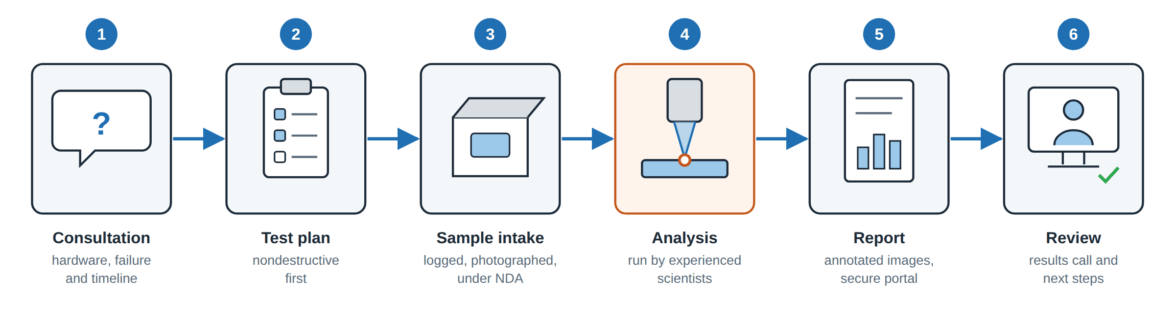
- Consultation: the hardware, the failure or question, and your timeline.
- Test plan: nondestructive inspection first, then targeted cross-sections and chemistry.
- Sample intake: logged, photographed and handled under NDA.
- Analysis: by experienced scientists.
- Report: annotated images and data in your secure portal.
- Review: a results call with the scientist who ran the work, and next steps.
Techniques for Data Center and AI Hardware Analysis
| Area | Techniques | What you learn |
|---|---|---|
| Nondestructive inspection | 2D X-ray, micro-CT, scanning acoustic microscopy | Voids, cracks and delamination in packages, TIM layers and boards |
| Cross-sections and microscopy | Mechanical cross-sections, SEM, FIB-SEM, optical microscopy | Microbumps, hybrid bonds, solder joints, vias and plating |
| Atomic-scale imaging | TEM, STEM-EDS/EELS | Interfaces, barrier layers and bond quality at the nanometer scale |
| Surface chemistry | XPS, ToF-SIMS, Auger | Contact films, corrosion products and contamination on pads and connectors |
| Trace and fluid chemistry | ICP-OES, ICP-MS, ion chromatography, FTIR, GC-MS | Dissolved metals, ions and breakdown products in coolants, and residues on hardware |
| Thermal and mechanical | TMA, DSC, TGA, DMA, nanoindentation | CTE, Tg, cure and modulus of underfills, mold compounds, substrates and TIMs |
| Electrical | Nanoprobing, 4-point probe | Device-level electrical behavior and sheet resistance |
See also our Semiconductor, Photonics and Energy & Batteries pages for chip-level, optical and backup battery work.
From R&D to Production
- R&D and material selection: compare TIMs, underfills, substrates and cooling materials before you commit.
- Process development: measure how changes to bonding, underfill, TIM application or plating affect the part.
- Package and board qualification: inspect and cross-section parts before and after reliability testing run by you or elsewhere.
- Supplier and incoming checks: verify materials, platings and coolants lot to lot.
- Deployment: track coolant chemistry and corrosion in running systems over time.
- Failure analysis: find the root cause of field returns from accelerators, boards and cooling hardware.
Enterprise Metrology Solutions for Data Centers and AI
Chip designers, server makers and data center operators bring Covalent's scientists into their hardware programs: package and TIM qualification, cooling material compatibility studies, coolant monitoring and failure analysis of fleet returns. Extra FIB-SEM, TEM and acoustic microscopy capacity is there when a launch or a field issue fills your own lab.
Experts on your team
A technical lead who joins your hardware and reliability reviews and knows your packages, boards, cooling designs and earlier failures.
Methods development
New methods for new packaging and cooling technologies, such as hybrid bonds, new thermal interface materials and immersion fluids.
Lab on demand
Extra inspection and failure analysis capacity during qualification, a new platform launch or a spike in field returns.
One partner, secure data
Package, board and coolant analysis in one lab, plus Covalent Connect partner labs, under ISO/IEC 17025, SOC 2 and ITAR, with results in a secure portal.
Data Center & AI Testing Services at Covalent
Our Sunnyvale lab runs nondestructive inspection, cross-sectioning, FIB-SEM, TEM, surface analysis and trace chemistry under one roof, so a failed accelerator, board or cold plate can go from inspection to root cause with one team. You work directly with the scientists running your samples, and results arrive in a secure portal. Covalent is accredited to ISO/IEC 17025, holds a SOC 2 examination and is ITAR registered. For techniques we don't run in-house, we can place work through Covalent Connect, our network of trusted partner labs.
Turnaround is typically 5–7 business days, with rush options available at an extra cost.
Frequently Asked Questions
Can you analyze a failed GPU or AI accelerator?
Can you inspect HBM stacks and hybrid bonds?
Can you check thermal interface material coverage?
Do you measure thermal conductivity?
We don't run thermal conductivity measurements in-house. Ask us about arranging them through Covalent Connect, our network of trusted partner labs. We characterize the TIM's composition, filler and structure to explain the results, so you have one point of contact.
Can you analyze our liquid coolant?
Do you test materials for immersion cooling compatibility?
Yes. We compare polymers, elastomers, adhesives and board materials before and after exposure to your fluid with FTIR, GC-MS, DSC, TGA, hardness and tensile testing to show swelling, leaching and property changes. The exposure soak can run in your lab or ours.