
What We Offer
- R&D support and process development for thin films, waveguides and epitaxial layers
- Waveguide and device structure imaging and metrology
- Thin-film thickness and optical constants (n and k)
- Defect, strain and emission analysis in active materials
- Optical coating characterization
- Contamination analysis on optical surfaces and facets
- Failure analysis of photonic devices and assemblies
Why Teams Choose Covalent
Speed
Electron microscopy, optical spectroscopy and surface analysis run on the same device in one lab, so samples never ship between vendors.
Quality
Optical constants from ellipsometry are often cross-checked with UV-Vis-NIR, and cross-sections confirm what surface imaging shows.
Detailed reporting
Reports that link materials data to device performance, so you know which process step to change.
Why Materials Analysis Matters in Photonics
In photonic devices, a few nanometers of sidewall roughness, a thin contaminant film or a crystal defect can scatter light, shift wavelength or shorten device life. Materials analysis finds those problems at the scale they happen and links them to device performance.
Common Challenges We Solve
| Challenge | What we measure | Techniques |
|---|---|---|
| Waveguide geometry and roughness | Width, height, sidewall angle and roughness | SEM, FIB-SEM, TEM, AFM |
| Thin films and coatings | Thickness, refractive index n, extinction coefficient k | Spectroscopic ellipsometry, UV-Vis-NIR, XRR |
| Active material quality | Defects, strain, bandgap and emission | Photoluminescence, cathodoluminescence, Raman, XRD |
| Optical contamination and defects | Particles, films and scratches on optics and facets | Optical microscopy, SEM-EDS, ToF-SIMS, XPS |
| Interfaces and bonding | Bond-line quality, voids, interface chemistry | Cross-sections, SAM, TEM, XPS |
| Surface topography | Roughness and form of optical surfaces | White light interferometry, LSCM, AFM |
How We Work With You
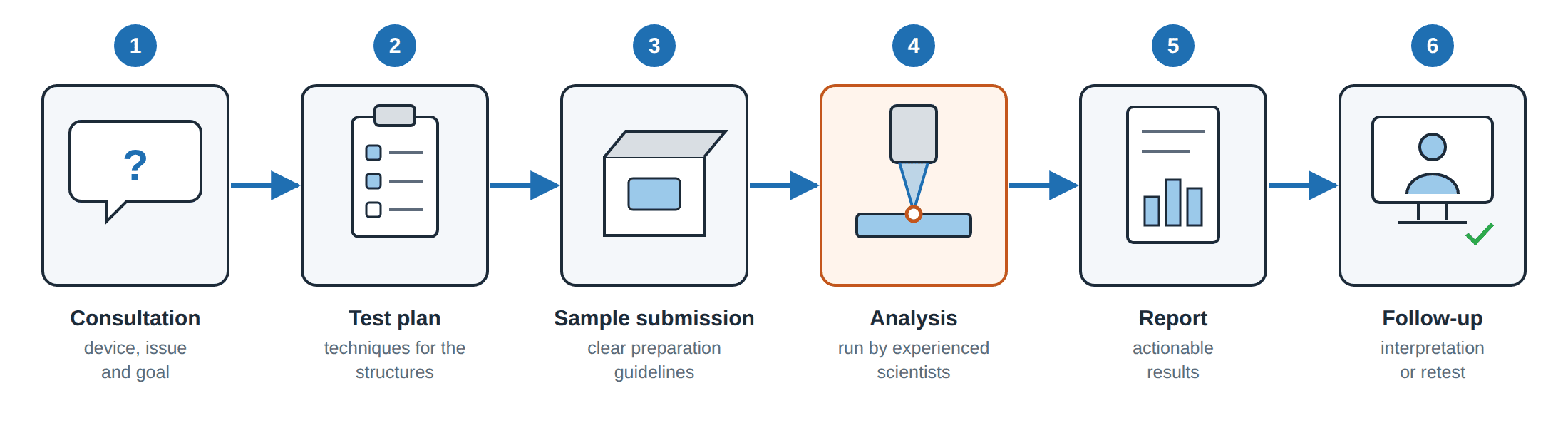
- Consultation: the device, the performance issue and your goal.
- Test plan: the techniques suited to the structures and materials involved.
- Sample submission: clear preparation guidelines.
- Analysis: run by experienced scientists.
- Report: results in an actionable format.
- Follow-up: an interpretation session or retest if needed.
Techniques for Photonic Device Analysis
| Area | Techniques | What you learn |
|---|---|---|
| Structure and interfaces | SEM, FIB-SEM, TEM, STEM-EDS | Waveguide geometry, layer stacks and interface quality |
| Topography | AFM, white light interferometry, LSCM | Sidewall and surface roughness |
| Optical properties | Spectroscopic ellipsometry, UV-Vis-NIR | Thickness, n and k, transmittance and reflectance |
| Emission and defects | Photoluminescence, cathodoluminescence, Raman, SNOM-Raman | Bandgap, defects and stress |
| Composition | XPS, ToF-SIMS, dynamic SIMS | Surface chemistry, contamination and dopant profiles |
| Crystal structure | XRD | Epitaxial quality, strain and composition |
From R&D to Production
- Material and process development: characterize new films, waveguide materials and epitaxial layers.
- In-process monitoring: measure film thickness, optical constants and dimensions on test wafers.
- Incoming component verification: confirm coatings and materials from suppliers meet specification.
- Reliability support: examine devices after aging or stress testing run elsewhere.
- Failure analysis: find whether a failure comes from a material defect, contamination or an integration flaw.
Enterprise Metrology Solutions for Photonics
Photonics companies use Covalent's scientists as an extension of their process and failure analysis teams, from thin-film and waveguide development through incoming component checks and failure analysis of returned devices.
Experts on your team
A technical lead and scientists who join your process and failure analysis reviews and know your waveguides, films and device structures.
Methods development
New methods for new film stacks, waveguide materials, epitaxial layers and bonding processes.
Lab on demand
Microscopy and optical analysis capacity during process development, ramp or a failure investigation, without adding instruments or staff.
One partner, secure data
Structure, optical and surface analysis in one lab, plus Covalent Connect partner labs, under ISO/IEC 17025 and SOC 2, with results in a secure portal.
Photonics Testing Services at Covalent
Our Sunnyvale lab combines electron microscopy, optical spectroscopy and surface analysis under one roof, so structure, optical properties and chemistry can be measured on the same device. Our scientists help you link materials data to device performance and decide what to change. For techniques we don't run in-house, we can place work through Covalent Connect, our network of trusted partner labs.
Turnaround is typically 5–7 business days, with rush options available at an extra cost.
Frequently Asked Questions
Can you measure waveguide sidewall roughness?
Can you measure refractive index of thin films?
Do you test laser or transceiver performance?
Can you find contamination on a laser facet or lens?
Can you characterize defects in active materials?
Yes. Photoluminescence, cathodoluminescence, Raman and XRD measure bandgap, defects, strain and emission.
Can you inspect bond lines in photonic assemblies?
Yes. Scanning acoustic microscopy finds voids, and cross-sections, TEM and XPS show bond-line quality and interface chemistry.